This thread has been locked.

If you have a related question, please click the "Ask a related question" button in the top right corner. The newly created question will be automatically linked to this question.

TLV7011: Mismatch Between Designed hysteresis and Measured Hysteresis

Part Number: TLV7011

Hi Team,

I designed a comparator with Vil=910mV and Vih=918mV .When I measured the hysteresis after simulation I obtained a value of 28mV.

The internal Hysteresis of the IC is 14mV and external is 8mV. As per my understanding these two will get added(Please correct me if I am wrong).

Then also the value expected is 22mV.May I know from where the extra 6mV is coming.

If you can tell me how to calculate the total hysteresis it will be helpful for me.

Please find the attached TINA file

Regards

hari

Comparator [TLV7011].TSC

  • Hi Hari,

    you should take into account the manufacturing tolerances of hysteresis and input offset voltage. If your programmed hysteresis isn't much bigger than the sum of hysteresis tolerance plus input offset voltage tolerance, the real thresholds will considerably differ from the calculated values. See also section 8.1.2 of datasheet.

    Kai

  • Hari

    I will review the simulation and model tomorrow and get back to you.

    To Kai's point, there is quite a variance in hysteresis over temperature (1.2mV to 14mV).

    Simulation models are generally based on the typical value which is 4.2mV in this case.

    So I will need to investigate why simulation shows so much greater.

    Chuck

  • Hari

    As I suspected, the model had a problem with how hysteresis was implemented.  I have corrected the model and attached a new TINA file for you to simulate with.  I have also attached an Excel spreadsheet that you can use to create new designs in the future.  Essentially the spreadsheet does the math for creating a comparator circuit with hysteresis.  Please note my previous comment about TI models using typical values, not max values.

    Here is our design guide for adding external hysteresis that includes the equations that are implemented in the spreadsheet.

    www.ti.com/.../sboa313a.pdf

    Next week I will get the model corrected on ti.com.  Sorry for the confusion that the model created.

    Chuck

    Comparator_hyst_tool.xlsx

    TLV7011_chuck.TSC

  • Hi Chuck,

    Thank you very much.

    Sorry for the Delay in response,I was in a vacation.

    Could you please explain me the below thread.

    I did not understand properly the second relation he is explaining in the below thread.(offset voltage and Hysteresis).

    How I will be able to check that.

    Regards

    hari

  • Hi Hari,

    what exactly didn't you understand?

    The input offset voltage of comparator just shifts both the trip points by the same amount.

    Kai

  • Hari

    Kai has summarized it well.  Let's make an example to explain.  Let's assume we build a circuit where we use and ideal comparator with 0mV offset and we design the switching thresholds with external hysteresis to be +5mV and -5mV.  Now let's assume this is a non ideal comparator that has an offset of +2mV.  The new switching thresholds would be +7mV and -3mV.  The total hysteresis is still 10mV but due to the offset, it is unsymmetrical around 0V.

    Hope this helps,

    Chuck

  • Hi Chuck and Kai,

    Thank you very much.

    According to the above example comparator's offset voltage is added to the external Hysteresis,but the total Hysteresis remains the same.

    But comparator's will have both offset voltage and internal hysteresis .

    My question is both the internal hysteresis and offset voltage will added to external hysteresis.

    Thanks & Regards

    Hari

  • Hari

    My simple example explains the relationship between internal hysteresis and offset. These values would need to be used as the switching thresholds in application note that I shared previously. External hysteresis is added by using the offset and internal hysteresis to calculate the appropriate feedback resistance.

    Sorry for originally making it seem simpler than it is. You need to do some algebra or use the spreadsheet I provided to design external hysteresis.

    Chuck

  • Hi Chuck,

    Thank you very much.

    I will do as per your suggestions,will contact you if any help is required.

    Regards

    Hari

  • Sounds good Hari.  Good luck.

    Chuck

  • Hi Chuck,

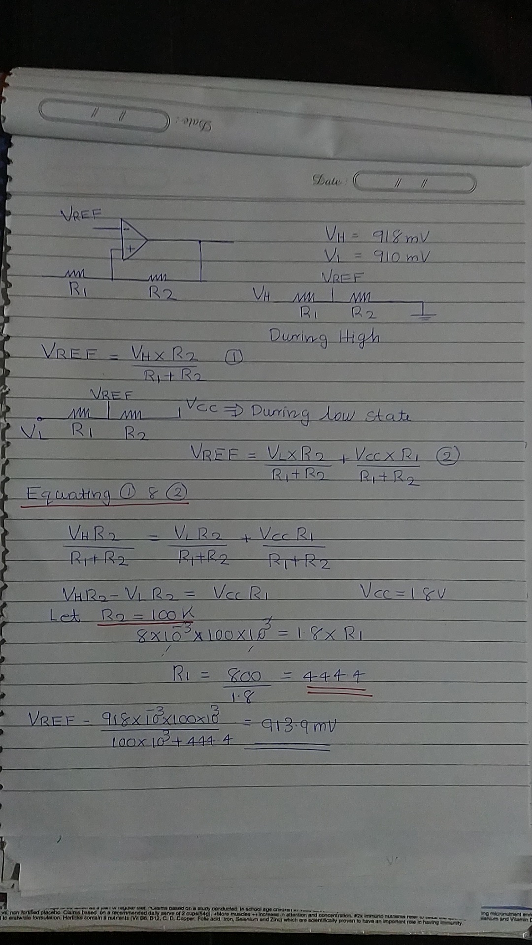
    I tried to calculate the component values according to the application note provided by you.

    I set R2=100K and Calculated R1 and obtained a different value.According to calculator R1 value is 221,but I obtained 444.4.

    But the voltage required at inverting terminal is correct.

    I am attaching my calculation sheet along with this.May I know where I went wrong.

    Regards

    Hari

  • Hari

    There is nothing wrong with the calculation you are showing me.  I am not sure where you are getting 221 from, but your math is correct.

    Chuck

  • Hi Chuck,

    When I put my Vh(918mv) and Vl(910mv) in the excel calculator I am getting R2=100k and R1=221.

    In the above calculation I fixed R2=100K and tried to find R1 but its value is different from that obtained from the calculator tool

    Regards

    Hari

  • Hari

    Are you sure that you selected the option for PP output stage and NON Inverting Comparator configuration?

    When I used the tool, I do not get R1 = 221.  Anyhow, your math is correct.  The Excel tool calculates for R4 and R5 assuming you do not have a dedicated REF.  The important thing is that the analysis you shared is correct. 

    Here is a copy of the tool again with your values entered.  Maybe this will help show what is different.

    Chuck3365.Comparator_hyst_tool.xlsx

  • We have not seen any response on this thread for a while, so I will be closing the thread.

    If you need further assistance, please feel free to reopen or start a new post.

    Thanks

    Chuck