This thread has been locked.

If you have a related question, please click the "Ask a related question" button in the top right corner. The newly created question will be automatically linked to this question.

TLV2771: TLV2771, Signal Conditioning Piezoelectric Sensors,note SLOA033A , what's the difference between voltage mode amplifier and charge mode amplifier

Part Number: TLV2771

hi 

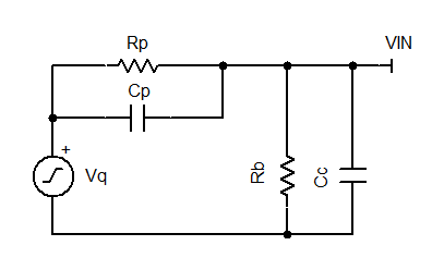
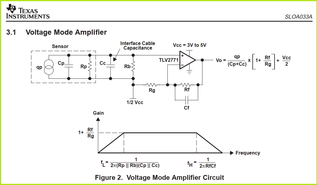
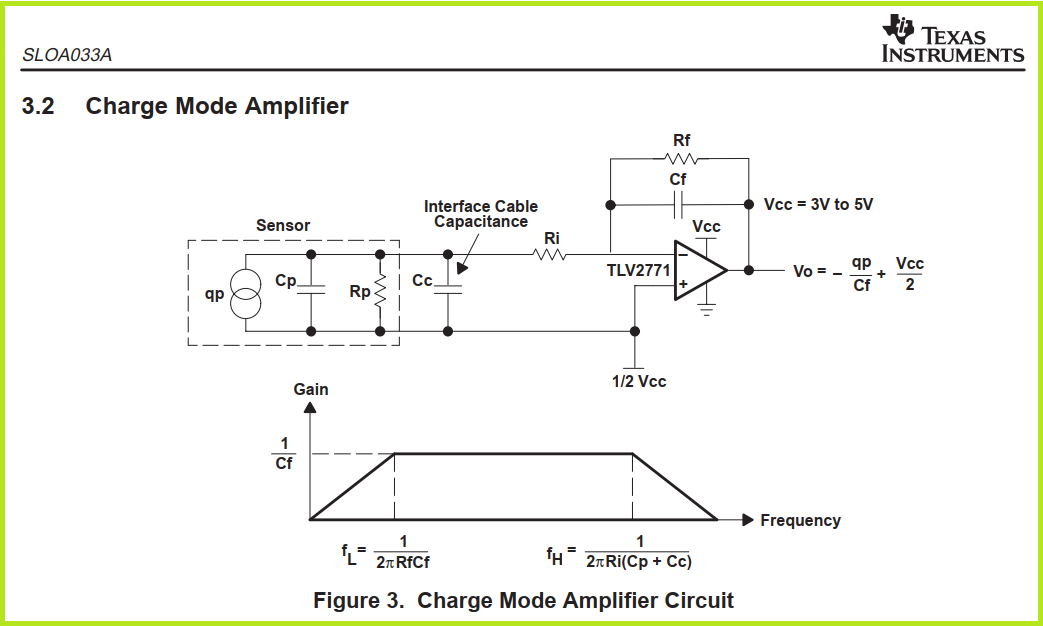
There is the question. In this document,http://www.ti.com/lit/an/sloa033a/sloa033a.pdf, I cannot tell the difference between voltage mode and charge mode. Why we can only consider Cf on charge mode and ignore Cp and Cc?

  • Hello Andy, 

    Welcome to the e2e forums.

    The section 2 charge and voltage models are a simple conversion between Norton and Thevenin models.

    Which formula only considers Cf and not Cp,Cc ? 

  • HI

    In the data sheet, it shows that in voltage mode amplifier, the Vout should be consider as Vo =[qp/(Cp+Cc)]x[ 1+ Rf/Rg]+Vcc/2. On the other hands, the Vout of charge mode amplifier should be consider as 

    Vo =-qp/Cf +Vcc/2. What's the difference between these mode. Can I just design my circuit into "charge mode amplifier" so that I can only consider Cf rather than Cp and Cc?

    thanks


  • Andy,

    Voltage mode actually makes the equations more complicated. Both capacitors and both resistors are still there, but now they are voltage dividers.

  • Hi Andy,

    the formula in figure 2

    says that the sensor charges the parallel circuit of Cp and Cc and that this voltage is amplified by the TLV2771 forming a non-inverting amplifier. Remember that the capacitance is defined by the formula C = Q / U. Equivalent transformation results in U = Q / C, finally.

    The formula in figure 3, on the other hand,

    says that the parallel circuit of Cp and Cc isn't charged by the sensor. Only Cf is charged. But this is only true, if Ri negligibly small, or by other words, if the -input of TLV2771 sits on virtual ground (here 1/2 Vcc)!!

    If Ri cannot be neglected, on the other hand, the signal current from the sensor will cause a voltage drop across Ri which will force the parallel circuit of Cp and Cc to be partially charged. The application note should have mentioned this fact.

    It's important to note that the specific advantage of the charge sensitive amplifier compared to the standard voltage amplifier is just that the signal input sits at virtual ground. By this the cable capacitance Cc isn't charged by the signal and does not play any relevant role! The sensor only sees a very decreased capacitance, actually Cc / "loop gain". But, again, only if Ri is negligibly small...

    Kai

  • Kai,

    Is Ri needed at all? In the formulas, only fH is affected. A later stage could perform the low pass (high block) function.


  • Hi Ron,

    you are right, Ri isn't needed for the charge sensitive amplifier at all. The appnote mentions Ri only as ESD protection...

    Kai