This thread has been locked.

If you have a related question, please click the "Ask a related question" button in the top right corner. The newly created question will be automatically linked to this question.

TLV7031: TLV7031 Output is not going to Vcc

Part Number: TLV7031
Other Parts Discussed in Thread: TINA-TI, TLV3491

Dear Team,

I am using TLV7031 for one of my applications.

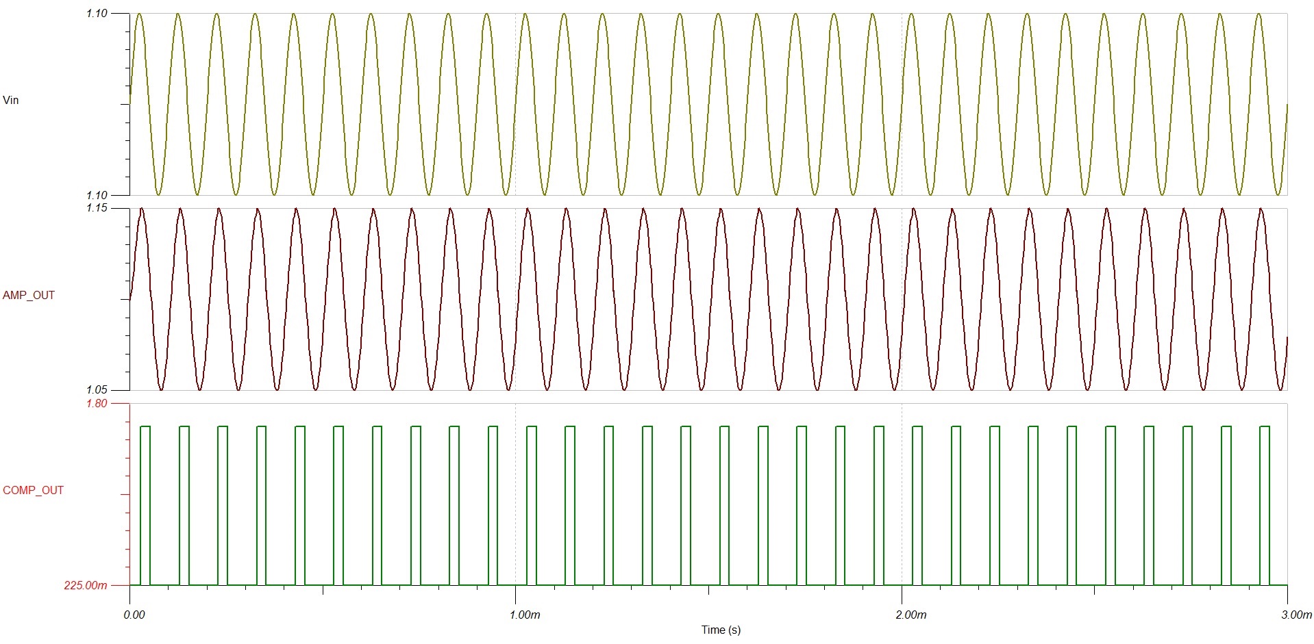
TLV7031 is powered with 1.8V, but during the high state, it is only going to 1.6V. May I know why it is happening like this.

Please find the attached TINA simulation file and Output waveforms.

Regards

hariMAX9914 - TLV7031DPWR.TSC

  • Hello Hari,

    You are most likely experiencing an output swing limitation. See section 6.8 of the datasheet, the TLV7031 can only swing within about 0.2V of the rail at +5V. This theoretically depends on the output current, as shown in Figures 18 and 19. In the TLV model macro, this is modelled in part as

    XIVOH VCC VOH VIMON OutputCir_VOHVOL PARAMS: VSUPPLYREF=5 VOUTvsIOUT_X1= {ABS(0)}
    + VOUTvsIOUT_Y1=4.8 VOUTvsIOUT_X2= {ABS(10e-3)}  VOUTvsIOUT_Y2=4.8

    Technically for a +1.8V supply you should be able to get closer to the rail than 0.2V, but you can see by shifting the supply of U2 that the output always tracks within 0.2V of the rail, even though the output current is very low (~10uA maximum in the provided simulation). I believe this is really more of a model limitation than a reflection of how the unit would perform in the real world - Figure 18 is more accurate in that regard.

    Cheers,

    Jon

  • Hi Jon,

    Thank you very much.

    What I understood is because of simulation model issue it is not coming proper 1.8V.

    But in real board I will get almost 1.8V for High state.

    Regards

    Hari

  • Sorry Hari

    I see the problem with the model that you have discovered.  We will work on getting that fixed next week.

    In the meantime, Jon's comments are totally valid.  You will get nearly ideal swing to each rail with your 100k feedback load.  The drop should be less than 10mV.

    Chuck

  • Sorry Hari

    we are still working on getting all of the models related to this family updated.  Hopefully we will have all of the TLV70xx models resolved by next week.  Unfortunately, they all have the same problem.  In the meantime, I hope you were able to proceed with your application.

    At this point I presume that you don't have any further application questions regarding your circuit.

    Chuck

  • Hi Chuck,

    No issues. Please take your time.

    Regards

    Hari

  • Thanks Hari for your patience.

    Chuck

  • Hi Chuck,

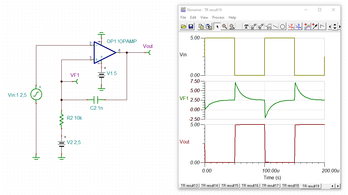
    I saw one reference circuit in TINA-TI called "Comparator With AC Hysteresis" (https://www.tina.com/blog/comparator-with-ac-hysteresis/)

    I did a google search for finding how to design the same but did not find anything.

    May I know how to set thresholds in these circuits

    Regards

    Hari

  • Hari

    AC hysteresis is positive feedback with a capacitor instead of a resistor.  It is built on the principle of no instantaneous change in voltage across a capacitor.  So when the output of the comparator goes high with a capacitor feedback, a similar step is seen at the non-inverting input.  I think of ac hysteresis as a way to clamp the output of the comparator.  The initial threshold is set as if there is no capacitive feedback.  Only when the output transitions do you get a dramatic shift in the non-inverting input.  Honestly, I have not found this implemented very frequently.  Why do you think you need to implement in this way?

    Chuck

  • Hi Chuck,

    Thank you very much.

    I saw this circuit accidentally. I never see this type of comparator circuits in any books.

    Due to my curiosity, I searched on the web to know more about this, but could not find anything.

    I won't be implementing this circuit in my present system.

    May I know is it possible to set thresholds(Voh, Vol) using this circuit.

    Regards

    Hari

  • I can imagine that you could.  It just gets more complicated to implement because you now need to take in account how the non-inverting input voltage will dissipate charge once the output has transitioned and passed its transition to the non-inverting input.  Imagine a comparator that transitions from 0V to 5V on the output and has a capacitor feedback to the non-inverting input.  The input will see a 5V increase from what it was previously.  This would be seen as a very dramatic amount of hysteresis and could hold the output high for an indefinite amount of time.  The amount of time would be dependent on the discharge of the voltage that is transferred to the non-inverting input.  I have never seen equations derived. It would be very design specific but that is the principle behind how it would work.

    Most of the time, 10's to 100's of mV of hysteresis are sufficient for an application, so having this sort of ac hysteresis is not commonly implemented.  Sorry, but that is about all I can offer as an explanation.

    Chuck

  • Hi Chuk,

    Thanks :)

    Regards

    Hari

  • Hi Hari,

    a comparator with AC feedback via a capacitor has some severe disadvantages. That's the reason why it is seldom found in the electronic world.

    As Chuck already mentioned, the feedback capacitor is very quickly and very largely charged when the comparator output toggles. So, the voltage at the +input of comparator either exceeds the absolute maximum common mode input voltage range (if it does not contain an input protection circuitry) or the existing input protection circuitry has to withstand very high current pulses.

    The first simulation shows the behaviour of a rather ideal comparator without containing an input protection circuitry:

    You can clearly see the overvoltage and undervoltage glitches at the +input.

    The next simulation shows a comparator (TLV3491) containing ESD proteczion diodes:

    You can see the clamping effect of input protection circuitry and the large current pulses. Large current pulses during the comparator switching is what we try to omit, because this will generate ground bounce and ground noise which can destabilize the comparator. That's why we also don't want to have big capacitive loads at the output of comparator.

    The only reason for adding a small cap from the output to the +input of comparator can be the wish to compensate for the influence of too large stray capacitance from the +input to signal ground which causes an unwanted phase lag. Then, a feedback capacitor can act as a phase lead compensation to speed up and stabilize the comparator. This phase lead compensation works like it can be seen in scope probes or compensated voltage dividers: The time constant of lower resistance and paralleled capacitance (stray capacitance producing phase lag) should equal the time constant of upper (hysteresis) resistance and paralleled "phase lead" capacitance. Sometimes the upper (hysteresis) resistance is even omitted and only the (phase lead) capacitance can be seen.

    Kai 

  • Hi Kai,

    Thank you..

    Regards

    Hari

  • Thanks Kai and Hari

    I will be closing this post now.  If support in a new area is required, please open a new post.

    Chuck