This thread has been locked.

If you have a related question, please click the "Ask a related question" button in the top right corner. The newly created question will be automatically linked to this question.

THS3001: Alternative op amp requiring only single supply (+5V) for use on the THS5671EVM

Part Number: THS3001
Other Parts Discussed in Thread: THS5671A, , LMH6723, THS4271, OPA695, THS3215, THS3217, OPA837

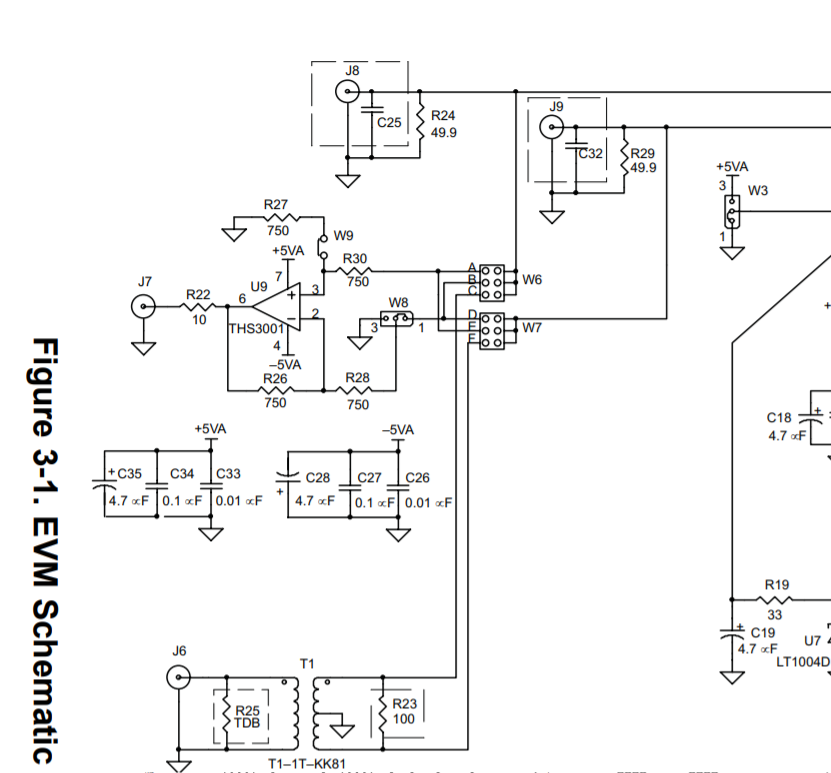
I'm hoping to use the THS567EVM to convert from an FPGA output to custom analog input board, but we are using single supply (+5V) for all our components. The DAC THS5671A is specified for 5V analog supply as well as +/-5V, but the eval module appears to need the dual supply due to the THS3001 op amp requirements. Is it possible to run the eval module from a single 5V supply using the given op amp? If not, is there an alternative that could be used in place? I also have a +2.5V supply for our op amp reference pins, if that's helpful.  

  • Hello Kendall,

    It is true that the THS3001 cannot be run at a single supply voltage of 5V. The only other pin-to-pin parts that might meet your requirements are the LMH6723 & THS4271. Here is a comparison chart of the three parts: 

    8176.Compare Parts.pdf

    If either part is used, you will probably have to reference the amplifier to mid-supply as to not exceed any input/output limitations.

    Best,

    Hasan Babiker 

  • Hey Kendall,

    I was looking at that EVM schematic (circa 2001) and it is already less than ideal from that groups early understanding of complementary to single ended DC op amp circuits. 

    This was before TI bought Burrbrown where they were not yet understanding that active impedance nature of the inverting side here - but whatever, this is what is in textbooks and has always been mistaken. I wrote an app note on that at one time,but lets not go there. 

    To operate a DC coupled complementary to single ended op amp on this board, a number of changes will need to be made. Definitely just dropping in another part is not going to work. - but just looking at what the THS3001 is (+/-15V CFA) a lower supply upgrade would be the OPA695. Staying with CFA on a single 5V supply is not going to have much swing as none are RR output (with one ADI exception, but its a dual DSL driver type part)

    Questions 

    1. Can you be AC coupled

    2. min max signal frequency range

    3. Normally these circuits come out through 50ohm, they have 10ohm now - what would you like to do and Vpp at final load

    Incidentally, since these early efforts we did quite a lot more on DAC interface solutions. If this is kind of lab work, you might consider ignoring the THS3001 path and just connecting the two 50ohm ground terminated path to the THS3215 EVM board - that part was intended for this function (a faster THS3217 is also there). Those will not be 5V solutions either, but will need +/-V supplies.

  • Hi Michael, 

    The output of the EVM is going to a buffer (ADA4851: https://www.digikey.com/product-detail/en/analog-devices-inc/ADA4851-1YRJZ-RL7/ADA4851-1YRJZ-RL7CT-ND/4166856), followed by a DC blocking capacitor prior to output to the load. To answer your questions: 

    Questions 

    1. Can you be AC coupled - Yes

    2. min max signal frequency range - 100Hz to 10MHz

    3. Normally these circuits come out through 50ohm, they have 10ohm now - what would you like to do and Vpp at final load - I'm not sure I understand the question, but max Vpp should be <2.5Vpp as the ADA4851 will be running 0-5V with a 2.5V reference. 

    I'm okay sacrificing speed or other specs to make this work in my system. Ultimately I'd like to implement the DAC (THS5671A) on my own board, but I figured starting with the eval module would be a good idea (maybe not if it's super complicated to make it fit in my system though....). What do you think? Am I making this unnecessarily hard?

  • Ok Kendall, 10Mhz is not much and 2.5Vpp is not much either, that will ask for about 80V/usec slew rate - many RRoutput choices there - 

    it is a difficult thing to pin down, but selecting and designing this kind of stage has a distortion suppression question hiding underneath it. The lower you want that, the more design margin (speed and slew rate) and design effort (balanced input Z to the DAC) you need to undertake - if you don't care about distortion, that relaxes things a lot. 

    The current THS3001 path is only intended to get a single ended version from the complementary DAC output - is that what you want? Are you going through a cable to the ADA4851? if so that gets into a doubly terminated 50ohm interface - if not, that 10ohm or something is intended to isolate the Cload for stability. 

    So, you might be able to do this with minimal changes to the existing circuit using a negative R input RRout part like the OPA837. I am not considering pin drop in right now, let the TI apps folks drill through that. 

    If you are going with the amplifier output, keep in mind those 50ohm to ground will set the DAC swing going into that diff to single stage, normally that output is expecting another 50ohm termination to give the DAC a 25 ohm load - make sure you consider that in setting up the gains. 

    If you just used the current circuit with the OPA837 and single 5V supply, the inputs will be ok swinging from ground up - the output cannot get completely to ground so normally we add a DC level shifting circuit to shift it up maybe to midsupply . That DC level might be ok directly to operate into the ADA4851. Or you might want a DC blocking cap series out into that with its DC reference set up over there. 

    Anyway, as I said there are many RR out 5V parts with enough speed for your app - those will all be VFA type, but should be fine.