This thread has been locked.

If you have a related question, please click the "Ask a related question" button in the top right corner. The newly created question will be automatically linked to this question.

INA317: Thermal cycling

Part Number: INA317

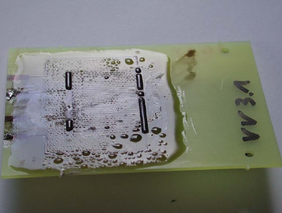
I am planning to perform repeated thermal cycling on on PCB mounted INA317,using following steps. I am planning to pot the  whole PCB in silicone to mitigate the temperature effects. 

a.            Warm up period.

b.            30 minutes at 138 degrees C, in ~2ATM steam atmosphere.

c.             Cool down period.

Preliminary, I am planning to test output voltage using known input voltage steps. What other parameters shall I pay special attention while evaluating the performance after thermal cycling.

  • Hi Jagbir,

    Questions:

    What other parameters shall I pay special attention while evaluating the performance after thermal cycling.

    Based on your thermal cycle test in INA317, it appears that this is non-operational thermal cycle test. The reasons that I am speculating is that no op amp components can handle temperature of 138C environment while it is in operating conditions (without some of kind of cooling, say cooling plate etc.)

    When you are doing thermal cycle tests, there are two main different types of thermal cycling tests (dynamic or static thermal temperature cycling tests). Regardless which one you are doing, here is what you need to be aware: 

    1. You have to perform the test in actual end product configuration. Potting the PCB with silicone compounds are not likely representative in your final product configuration. So you need to test the product as is, otherwise, your test result will not be valid. 

    2. All thermal cycling has to follow a specific compliance in industry. Automotive has its defined thermal cycling test requirements. Aerospace is doing slightly differently. Thermal cycling test in medical industry is not the same either. So I need to know which industry compliance you are doing, and you need to follow that particular thermal test standard and test methods and procedures. 

    3. The 138C for 38 mins seems to be high and long for high temperature operation, unless it is non-operational test. 

    4. I have been involved in HALT & HASS tests over 6 years, and your thermal testing parameters do not look familiar to me. 

    Here are a typical HALT & HASS test setup for thermal cycling test. 

    1. The HALT & HASS test chamber is required to have very high temperature ramp rate for heating and cooling, something like 60-80C/min for hating and cooling. The chamber is cooled by liquid nitrogren. HALT &  HASS chamber also has random vibration profile, though you are not using per the test. The chamber is required to high very high flow rate, otherwise you may have hot temperature location somewhere in the chamber. The heating or cooling air duct is supposed  to be placed directly on top of EUT (INA317) for the duration of the test. 

    2. Your monitored temperature sensors have to be placed on top of EUT. In this case, 1" above INA317 or directly on top of INA317 package. The INA317 package's temperature should be higher than air temperature of the chamber for INA317 operational test. 

    3. The operating temperature of INA317 is rated from -55C to +125C. The IC's Junction temperature is rated at 150C. By the way, these are typical temperature figures. Although the part has some kind of  thermal designed margins in INA317, not every part will meet the same thermal requirements. 

    4. If this is operational tests, you need to have a standard voltage rails, feed input signals to the input of the INA317, and monitor the output of the Op Amp over time and temperature. If INA317's power supply is part of the test, you need to record its voltage and current performances over time and temperature. The test need to reflect an actual thermal environment in a field. So keep all operating parameters as closely as possible for the test. 

    5. It is a good ideas doing the thermal tests in stages. In other words, you need to establish a baseline. Say the chamber temperature is set at 125C, you complete the thermal cycle test, and all parts are passed. Then you increase the chamber temperature to 132C, and repeat the same test. It may pass or fail the test. Since your baseline is 125C, then you can increment accordingly to the next thermal point. If it passed 132C thermal cycle test, then you can move on to the next thermal setpoint. At some point, you will see that the INA317 starts to fail or not working properly. As long as you keep the thermal test within the absolute maximum ratings, this is not a destructive test (It may stop working at some point). 

    6. If you have multiple INA317 samples, it is good ideas to perform these at the same time. 

    7. Since INA317 has mass, there will be a thermal lag during test. When temperature of the chamber is reached a setpoint, it may take INA317 op amp longer time to reach the chamber temperature. It seems to me that you are doing thermal soaking tests at 138C. It is not clear to me that 38 mins at 138C is the total test time at 138C or temperature ramp time + soaking time. The conventional thermal chamber can only do 2-10C/min, so to reach 138C from room temperature may take a while. Since your thermal test is not described in detail, I am unable to comment on it. 

    Anyway, I have written a lot here. If you have any additional questions. please continue to post on the thread. 

    Best,

    Raymond


  • Hi Jagbir,

    take care, silicon has a high water vapour permeability.

    Kai

  • Hi Jagbir,

    Question:

    I am planning to pot the  whole PCB in silicone to mitigate the temperature effects. 

    I forgot to address this "temperature effects: when you potting the INA317's PCB with silicon. 

    Silicon is good thermal insulator, however it is only good for short duration for conduction heat to reach INA317 inside of potting. In other words, by potting the PCB, you are delaying the heat transfer from the chamber to the INA317. If this is 38 mins temperature soaking test at 138, it may have other effects, such as it will take a long time to cool on the INA317.

    Silicon potting compound inside of the test chamber will gradually absorb the heat in the chamber. The Silicon compounds will reach a thermal equilibrium in the chamber due to thermal conduction, and INA317 will see near 138C in the end (may be higher due to heat dissipation of INA317). If you are doing more than one thermal cycling tests, the cumulated heat may trap inside of silicon compound and your INA317 will end up tested near higher temperature for entire cycling duration. During the cooling cycle, it will delay the cooling in INA317 as well.  

    INA317 will see slower temperature changes (rise or fall) over thermal cycling.  Perhaps, it may provide a better electrical performance characteristics in INA317. 

    Best,

    Raymond

  • I am not doing any measurements during the thermal testing. I will perform measurements only after cooling off the PCBs.

  • We are not doing any HALT/HASS test.We are planning to autoclave this part, the specification of which I have provided earlier.

  • Hi Jagbir,

    These test  configurations are very similar. Is the thermal test cycle non-operational or operational tests for INA317? It is not clear. You are still able to pass electrical signal to an autoclave, but your electrode connections are limited.  

    For autoclave test, you will need to place two or more temperature sensors next to INA317. In autoclave configuration, you have several testing issues. 

    1. Chamber's temperature uniformity is not very ideals, since the air flow inside of the chamber is none or minimum. Localized hot  temperature spot inside of the chamber may be an issue.

    2. The temperature ramp up time for autoclave is very long (unless you have a powerful heater outside), since it has a large thermal mass. It may take over 30 minutes to heat up the autoclave from room temperature to 138C. 

    For Non-Operational Test:

    You need to characterize your INA317's performance parameters before you placed the PCB inside of autoclave.  You characterize it again after completion of the thermal test, and looking for the differences or degradation of the part etc.. For INA317 non-operational test, the test setup is much simpler than operational test. 

    If your final product is supposed to be potted with silicon, then that is how you are going to test it. If it is not, test the PCB as is. It is still good ideas to establish your working performance/reference baseline at a given temperature, say 120C or so. 

    For Operational Test:

    Please follow my suggestions from the first reply.  

    Best,

    Raymond

  • Hi Jagbir,

    the photo shows water bubbles under a layer of silicon caused by air humidity:

    Kai

  • Raymond,

    Thanks for the detailed reply.Currently,  I am working on the test plan. I will reach out in the forum if I encounter any issues during this thermal cycling.

  • Kai,

    What were the ambient environment conditions during this test.

    Jagbir

  • Hi Jagbir,

    unfortunately only in German :-)

    Kai

  • Hi Jagbir,

    The Kai's suggested article is in German.  Kai is indicating that silicon compound has poor moisture permeability.  Water moisture will penetrate into silicon based potting compound in a humid condition (will not be ideal for humidity test or under high humid environmental application). The cumulated  moisture will precipitate onto a surface when the internal higher temperature is driving out the moisture from the potting material. So silicon compound is poor material to create the moisture barrier from an environment, if you want to keep INA317 in a stable operating environment. 

    One of better material to pot a circuit is using certain low permeability epoxy based compound, if you want to keep moisture away in a circuit. The issue with epoxy is that it will create stress during curing. These unwanted stress is not desirable for certain application. So you will need create a internal cavity or pocket that is free from potting stress (e.g., INA317), and only encapsulate the PCB's surrounding with epoxy.   

    Best,

    Raymond