This thread has been locked.

If you have a related question, please click the "Ask a related question" button in the top right corner. The newly created question will be automatically linked to this question.

INA118: Reducing Offset by taking REF pin 2mV below minus rail

Part Number: INA118
Other Parts Discussed in Thread: INA819, INA818,

Hi,

1) Is the only difference between the INA818 and INA819 the pin-out? The INA818 being a superior version of the INA118. Used with a MPX10DP Pressure Sensor.

2) The application is taking an MPX10DP differential pressure sensor (span is 0mV to 40mV)(subtracting the Pressure Sensor's DC Offset (20mV) - solved) and Differential-End to Single-End amplifying by 1000 to go into an ADC (span 0V to 5V). INA118 is on 0V to 5V rails. They want the INA118/INA818 to have a uni-polar output from 0V to 5V.

A big DC Offset issue was noticed with the INA118. That may be reduced by going to the INA818 (Unless you suggest something better).

But it go me wondering...

If I need to use a low impedance buffer to take the REF pin a few milli-volts below the V- rail (to reduce the DC Offset), will that definitely cause issues (or will that happen if the voltage is more like a diode drop?)?

The obvious answer is; that if you CAN take the REF pin below V-, then why don't you power the INA118 from the more negative voltage.

True, that's now what we will do on Rev 2.

But as I said, I was wondering.... 

Is a few mV - too much?

Cheers,

Peter

  • Hi Peter,

    can you post a schematic?

    Are you sure that the offset voltage issue is not coming from the pressure sensor?

    And yes, the both INAs only differ in the pin assignment:

    Kai

  • Hi Kai,

    Thanks - but I won't post a schematic.

    -----------------

    Yes, the pressure sensor has a ~20mV DC offset. Sitting on top of that is the pressure value from 0mV to say 40mV.

    I've managed to remove that DC Offset.

    ----------------

    This question is really about the INA on-substrate resistor network and my curiosity about taking the REF pin below V-.

    Figure 2) Optional Trimming of Output  Offset Voltage was what got me thinking about it.

    Figure 5) Single Supply Bridge Amplifier shows the REF pin at GND - same as the INA118 negative power supply.

    What would happen if you use Figure 2's trim method on Figure 5's power system.

    Regards,

    Peter

  • Hi Peter,

    what figures are you referring to?

    Kai

  • Hi Peter,

    Question:

    This question is really about the INA on-substrate resistor network and my curiosity about taking the REF pin below V-.


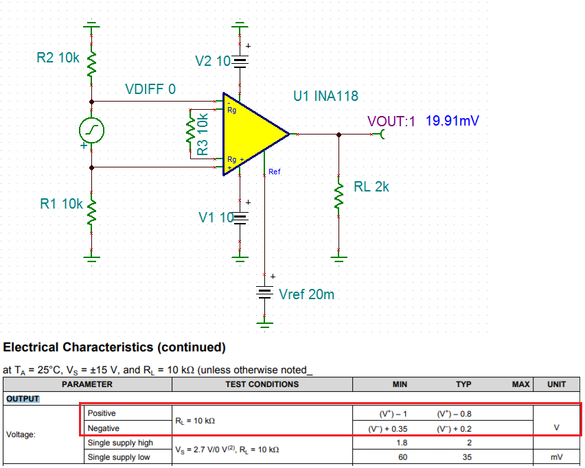
    When you shift Vref, you basically shift the output of INA118 by Vref amount, but the Vref shift needs to be within the V+ and V- supply rails. The INA118 won't operating in a linear region if you are taking the Vref below V-, see the output voltage requirements. 

    I had the same comments Kai indicated, which I am unable to figure out which Figure 2 you are referring. I saw Figure 5. Anwyay, I enclosed the Tina simulation below, and you can simulate the circuit per your issues. 

    Enclosed is INA118 simulation:

    /cfs-file/__key/communityserver-discussions-components-files/14/INA118--04272020.TSC

    Best,

    Raymond

  • Hi,

    Sorry about the references to various figures. I discovered the INA118 Data Sheet on my computer had been downloaded in 2009. The latest data sheet is very different.

    Regards,

    Peter