This thread has been locked.

If you have a related question, please click the "Ask a related question" button in the top right corner. The newly created question will be automatically linked to this question.

TLV4112: Oscillating

Part Number: TLV4112
Other Parts Discussed in Thread: TLV2772, TLV4111, , TINA-TI, LM7332, UA741

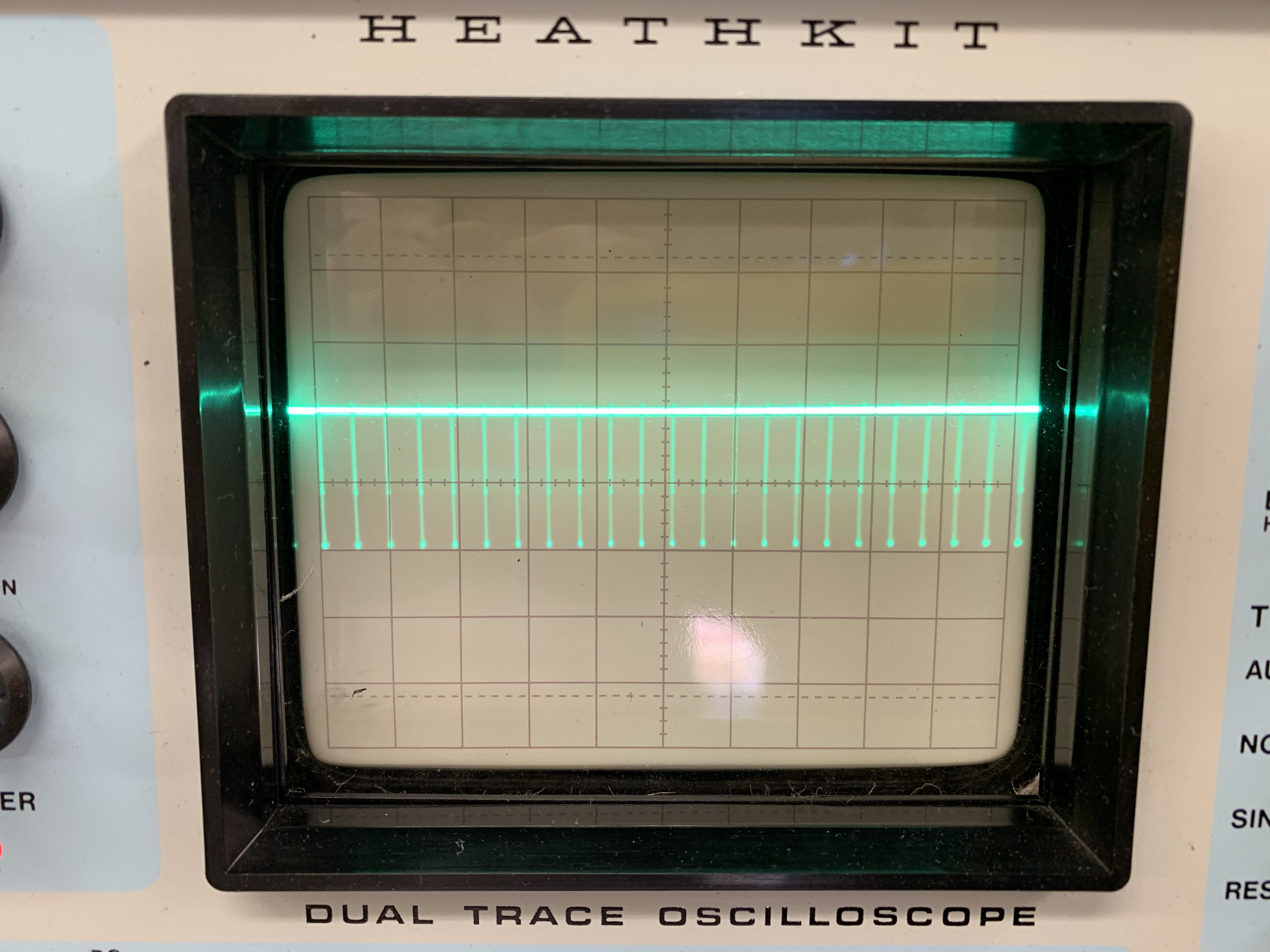
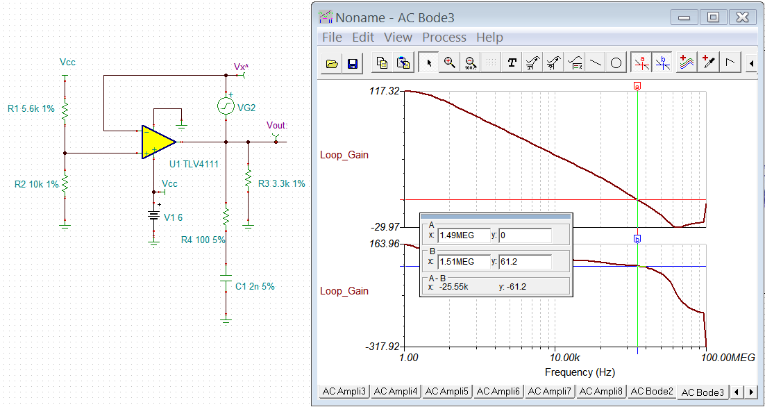
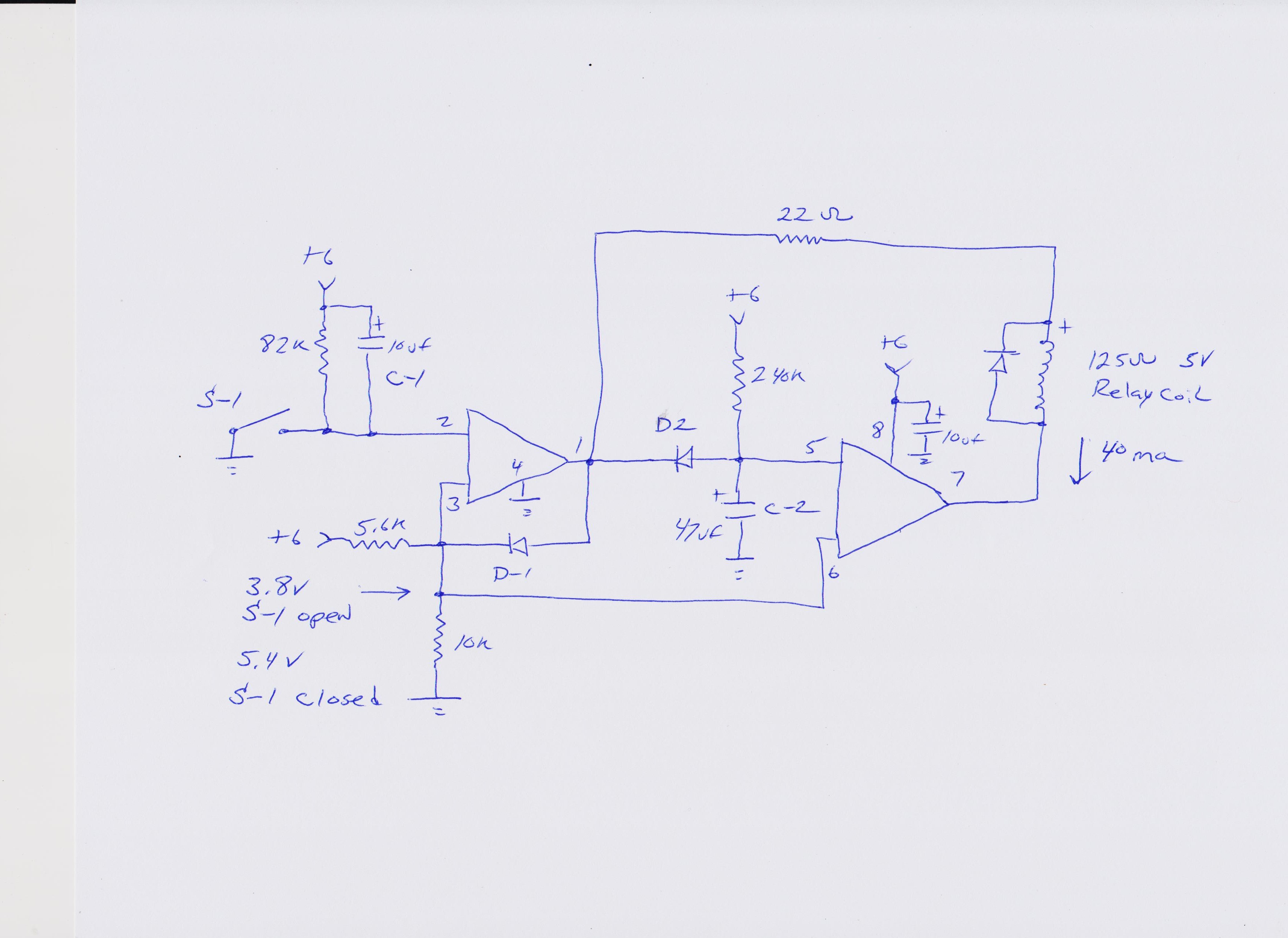
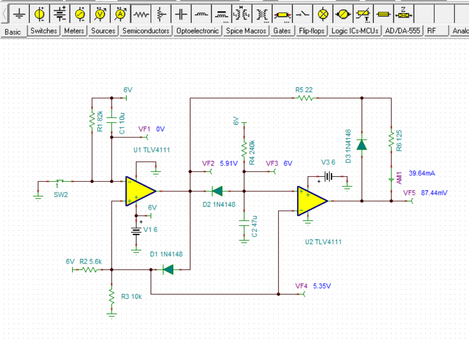
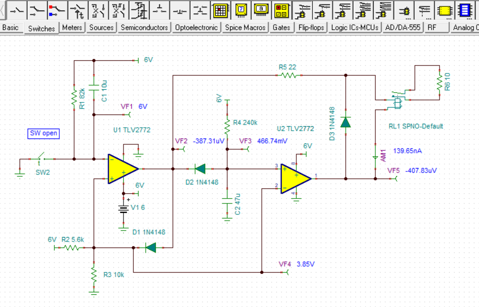
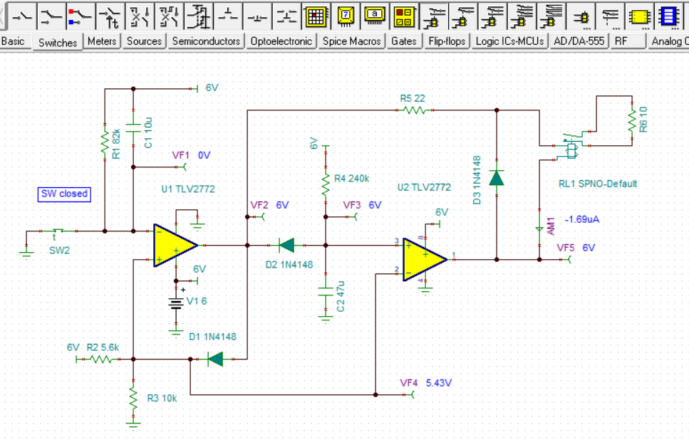
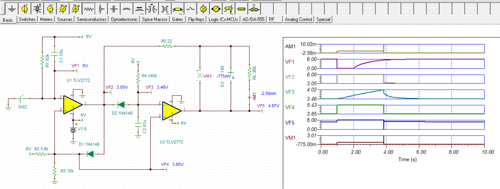
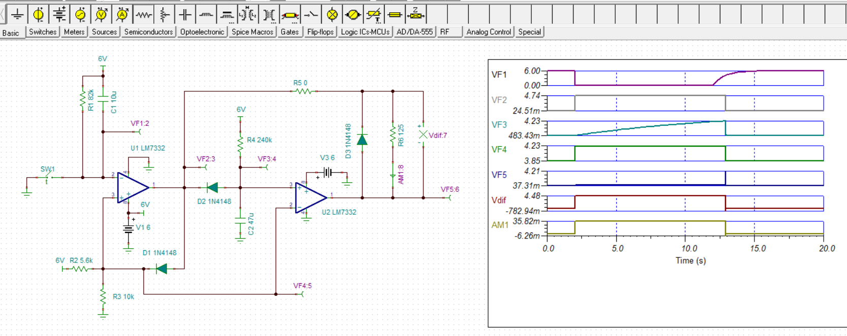
Purchased 2 of these TLV4112CP for a new design because the TLV2772CP could not drive my load.  MY design worked fine with the TLV2772 as long as the load was not heavy, regardless I never saw any oscillations with the TLV2772.  So when I put a TLV4112CP in the circuit it oscillates.  To try to figure where it was coming from so I tore the circuit down and built a test circuit as a voltage follower.  I put 3.8 volts on the + input and I get a series of pulses (oscillating) on the output.  I have never seen a OP amp oscillate with a gain of 1.  Power source is 6V single supply with a 10uf bypass right across the chip.  Seem like to me the issue is inside the chip with the design.  Can you shed some light on it? 

  • Well without a schematic kind of hard to guess,

  • Hi Larry,

    Can you present your schematic or image in the thread? It is difficult to visualize what you have. 

    Best,

    Raymond 

  • As prep, yes there is a 2019 updated TINA model, that is very useful to know, TLV4111.TSC

  • Hi Larry,

    I have never seen this behavior before from a TLV4112CP. It looks odd. What is the time scale on your oscilloscope? 

    You mention that you have left the second op amp in the package floating. That might be a problem if it is unstable under that condition. The preferred connection for an unused op amp section is to connect it as a buffer amplifier with the non-inverting input biased to a voltage within its linear operating range. You could use the resistive divider you have already set up for the op amp section you are using. Alternately, you could connect the unused buffer amp's non-inverting to ground since that is within its input common-mode voltage range. The output will be pushed up against the lower output rail in that case, but it unlikely to move off of it.

    Regards, Thomas

    Precision Amplifiers Applications Engineering

  • Hi Larry,

    In addition to Thom's comments. 

    The unity gain BW of the TLV4112 is approx. 2.4MHz. I simulated the model (TLV4111) from the above, and there is another pole (~4.1Mhz) at approx. one octave away from the unity gain BW, which it likely created this unstable behavior. In other words, there is 2nd pole at approx. 4.1Mhz region. 

    Anyway, please add the snubber circuit in parallel with 3.3 kOhm load, and it will likely resolve your problem, see the attached image. 

    Best,

    Raymond

  • OK, I have some light to shed on this.  I had both inputs of the unused section of the OP amp grounded.  I change it to a voltage follower and grounded the + input and that fixed the test circuit.  The repetitive rate of the oscillation was 50ns with the test circuit.  However, when I reconnected the actual circuit the oscillation is back.  I'm going to post the circuit below so you can see for yourself.  The strange thing is this circuit works perfect with the TVL2772 but that chip will not drive a 125 ohm relay.  This is why I switched to the 4112 for more drive current.  The circuit is very simple, just a short timer at C1 and a long timer at C2 using both sections of the OP amp as comparators.  If the short timer does not time out because S1 remained closed too long, then the long timer kicks in and turns off the relay because of differential drive.  What is happening is as the C2 charges from .6 via D2 to the rail the oscillations start at pin 7 just as the charge hits 4.5V.  In other words the 4112 OP amp is not functioning as a comparator very well, where the 2772 does.  With the hysteresis feedback via D1, the reference voltage on pin 6 shifts from 3.8 to 5.4 when switch S1 is closed. This is an intentional effect to increase the charge time of the C2 and creates hysteresis for S1.  The OP amp should not change states till the charge on the C2 gets to a tad over 5.3 volts, the reference.  It's going into oscillation just as the charge hits 4.5 volts on pin 5.  Why is the OP amp changing states before it gets to the reference voltage of 5.4 volts?  Your thoughts?  I reiterate, the TVL2772 does not have this problem with the same circuit.  I thought it would be a simple swap out. Apparently not. 

     be a simple swap out. Apparently not. 

  • Hi Larry,

    I have a suspicion the reason there is an issue with the TLV4112 in this circuit is because its positive common-mode voltage limit is being exceeded at both U1 and U2 when SW1 is one position or the other. The TLV4112 maximum VICR is VDD-1.5 V, or 4.5 V with the 6 V supply. Some op amps are more tolerant of a VICR over voltage condition than others. When I model your circuit I find that the U2 output is not changing state. When I substitute other op amps in the circuit and lower the relay load current the circuit functions as you describe. I believe if you can modify the design such that the VICR stays within the linear input range if the TLV4112 the circuit will function as expected.

    Regards, Thomas

    Precision Amplifiers Applications Engineering

    TLV4111_RelayDrv_01.TSC

  • That parameter you speak of must be specific to that OP only.  I've never seen an OP amp do that.  So if I put a 4.5 volt Zener diode on each minis input that should do it?  Or do I have to limit the + input to 4.5 volts max  too?

  • Hi Larry,

    I did some circuit simulations with the TLV2772 in place of the TLV4111 which you indicated worked well. The circuit does behave differently with the TLV2772, but it still doesn't appear to be functioning correctly. You can see what I am talking about from the two TINA-TI dc simulation screens seen below.

    In the first upper schematic the input switch is open and the output of U1 and U2 is very close to zero in both cases. They are slightly below 0 V and and that is likely due to the capacitor have a charge in the circuit. The notable point is that there is 0 V across the relay coil.

    In the lower schematic the input switch is closed and the output of U1 and U2 is at 6 V. Again there is 0 V difference across the relay coil. In both examples there is no appreciable current flowing through the relay path.

    If you follow the voltage levels from the simulations around the circuits they make sense. I have carefully viewed and drawn your schematic. Have I made a mistake in the way I have it in the simulation circuit, or is could you have misdrawn something in your schematic?

    Regards, Thomas

    Precision Amplifiers Applications Engineering

    TLV2272_RelayDrv_01.TSC

  • I'm waiting for a reply.  That parameter you speak of must be specific to that OP only.  I've never seen an OP amp do that.  So if I put a 4.5 volt Zener diode on each minis input that should do it?  Or do I have to limit the + input to 4.5 volts max  too?

  • Hi Larry,

    I posted the 3:48 am response about the TLV2772 simulation after you asked the question about limiting the TLV4111 input to + 4.5 V. The reason I posted that particular response about using the TLV2772 op amp is you had mentioned that the circuit had functioned correctly with that op amp. However, as I explained the simulation shows a problem where a ~0 V difference is seen across the load because the two op amp outputs are similar in voltage level throughout the timing cycle. This is evident from the timing diagram see below. VM1 is the difference voltage between the op amp outputs and it wouldn't be large enough to activate the actual relay coil.

    If I use the TLV4111 in place of the TLV2772 the circuit still doesn't work correctly in simulation. Limiting the TLV4111 input common-mode voltage to input voltage to the  +4.5 V is a good idea, but there still appears to be some underlying issue with the circuit design.

    Could you have a look at the schematic you sent us and my TINA circuit interpretation and see if there is a circuit connection issue in one, or both of them?

    Thanks, Thomas

    Precision Amplifiers Applications Engineering

  • Only thing I see wrong with your circuit is what I call SW1 you are calling SW2.  Also the values for R1 and R4 have to be changed for the 2772.  I used a 100K for R1 and a 1M for R4.  Those have to be changed for the 2772 because the load pulls down the output voltage too much affecting the hysteresis feedback. So the charge RC has to be altered to compensate for that to keep the same timing.   You have a 300 ohm load for RL.  I don't think you can get that 2772 to drive that load rail to rail.  I needs to be a much lighter load.  Let me ask you this, besides my suggestion to add the 4.5 volt Zeners to limit the input what would you do to make the circuit work correctly?  Or can you suggest a different number OP amp that will drive my 125 ohm load and allow the inputs swing to the supply without any side effects.  I had OP amp class in college and they never told us you need to limit the input voltage just as long as you did not go over the supply.  When you guys designed this 4112 you should of include voltage limits inside the chip so the customer could use the OP amp like most all OP amps I know of, which is, you can always let them go to the supply on the input without any side effects. This is a first I am learning about this undesirable side effect.

  • Hi Larry,

    I tried changing the input voltages from 6 V down to about 4.3 V while maintaining 6 V on the TLV4111 supply pins. The different node voltages changed the circuit behavior. Rather than spend anymore time on the TLV4111 I went to the TI website and looked for a high output current op that had supply rail-to-rail common-mode input range. I found an op amp in TI's General Purpose op amp line up that looks to meet all your circuit requirements - the LM7332. It features:

    • Wide Supply Voltage Range 2.5 V to 32 V

    • Wide Input Common Mode Voltage 0.3 V Beyond the rails

    • Output Short Circuit Current > 100 mA

    • High Output Current (1 V from Rails) ±70 mA

    I ran a simulation with the LM7332 in place of the TLV4111 and obtained what appears to be correct performance. I don't know what the timing is for the input switch so I used a switch that I could set an on time, and an off time. I used 2 seconds for the on time, and turned it off 10 seconds later. You can see the timing results. The 22 Ohm resistor in series with the relay col was dropped to 0 Ohms to reduce the voltage drop.

    By the way, input common-mode voltage limitations were present in the earliest of op amps such as the uA709 and uA741, and for many of the op amps that followed for decades. The TLV4111 was designed at the end of the last century so it is more so a legacy op amp. It is only in more recent decades that rail-to-rail input/output op amps have become reality. That has come about due to process technology and innovative designs. However, there are new op amps that have some common-mode input voltage limitations that come about because the design is maximizing some other very important characteristic and reasonable compromises are made. TI's Precision Labs - Op amps series has a section on op amp input and output limitations.

    https://training.ti.com/ti-precision-labs-op-amps-input-and-output-limitations-non-linear-behavior?context=1139747-1139745-14685-1138798-13960

    Regards, Thomas

    Precision Amplifiers Applications Engineering

  • OK on SW1 most of the time it is open.  However when activated it will go hi-lo repetitively at a rate of less than the RC of the first timer keeping the output at pin 1 high as long as the switch is active.  In the event SW1 gets stuck at a low the second timer will take over and open the relay.  That's a safety feature to prevent the device the relay is driving from overheating.  Most of the time the 2nd timer will be a non event. 

    I looked up the LM7332 and it looks like a surface mount.  I need a 8 pin DIP.  Does it come in a 8 DIP or will you have to make another choice?  I should of mentioned that.  Sorry.

  • Hi Larry,

    The LM7332 isn't available in the DIP. The DIP is being phased out and only older, legacy op amps may be available in that package.

    If your volume usage of the op amp is small, then an SOIC to DIP adapter may be a solution.

    Regards, Thomas

    Precision Amplifiers Applications Engineering

  • Guess then I will have to look for a different manufacture.

  • Hi Larry,

    Certainly. One of the other op amp outfits may have a comparable amplifier to the LM7732 in the PDIP.

    If you can close this e2e thread now I would appreciate it.

    Thanks, Thomas

    Precision Amplifiers Applications