This thread has been locked.

If you have a related question, please click the "Ask a related question" button in the top right corner. The newly created question will be automatically linked to this question.

INA180-Q1: About behavior of Vs pin’s voltage at shutdown

Guru 21045 points
Part Number: INA180-Q1

Hi Team,


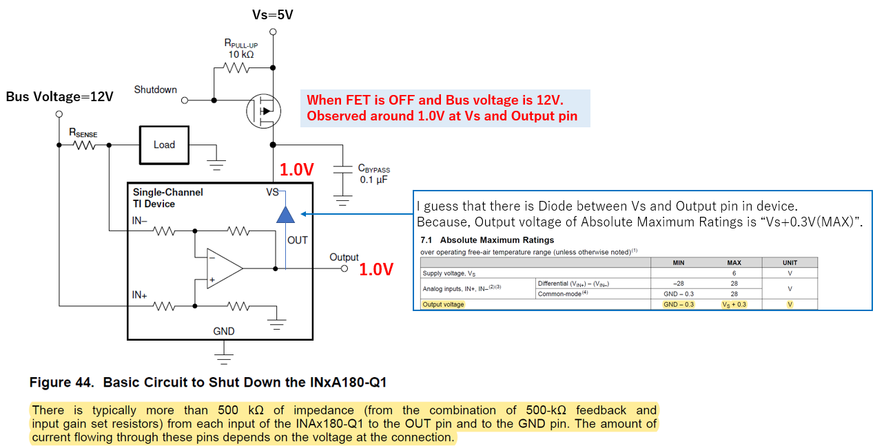
Our customer is evaluating INA180A3QDBVRQ1 at Figure44 circuit.

When FET is OFF and Bus voltage is 12V, observed around 1.0V at Vs and Output pin.

I guess that there is Diode between Vs and Output pin in device and it is correct behavior.

Is my understanding correct?


And, could you please let us know the workaround if you have any information(idea)?


Regards,

Hide

  • Hi Hide,

    Please add a 10KOhm load to ground if there is not one already; it should effectively eliminate the problem.

    Regards, Guang

  • Guang-san,


    Thank you for your reply and information.

    I guess that there is Diode between Vs and Output pin in device.

    Is my understanding correct?


    And, we added a 1KOhm (not 10kohm) load to ground.

    At the result, Vs voltage is decreased from 500mV to 30mV after ten minutes (very slowly).

    Therefore, they would to use the lower resistor value.

    Could you please let us know your recommended value if you have any idea?


    Regards,

    Hide


  • Hi Hide-san,

    There might be a diode as you drew, it is the body diode and will conduct when forward biased. In this device there is only ESD diode to ground, none from OUT to VS.

    I would think at least the output should quickly collapse to ground even with a 10KOhm. You may try a 10KOhm in parallel with bypass cap to bleed off residual charge. And see if it helps.

    Regards, Guang

  • Hi Guang-san,

    Thank you for your response.

    I’d greatly appreciate your verification.

    Regards,

    Hide