This thread has been locked.

If you have a related question, please click the "Ask a related question" button in the top right corner. The newly created question will be automatically linked to this question.

PGA113: output amplitude distortion

Part Number: PGA113
Other Parts Discussed in Thread: OPA333

Hi,

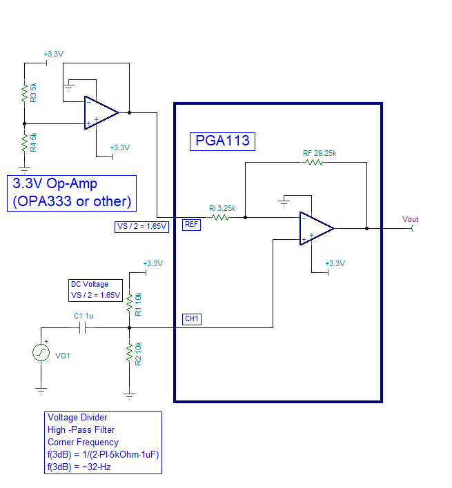
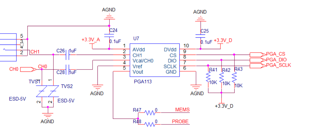
below is the schematic and outpu waveform:

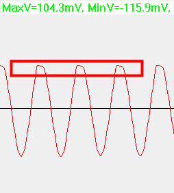
you can see that the postive amplitude of output is distortion. 

CH1 input :11.2~12mV 160Hz ; CH0/VCAL float ; Gain of CH1=10

why the postive amilitude distortion while negative is normal?

thanks.

  • Hi Betty,

    There are a couple of issues with the circuit.

    - The signal is AC coupled on the circuit above, where the capacitor C28 (1uF) is used as a DC blocking capacitor.  However, the DC input voltage at the PGA113 input is undefined since the input is floating and there is not DC signal Path at the PGA113 input. 

    If the signal needs to be AC coupled, the circuit needs to be modified, adding a voltage divider to set the DC bias point at the PGA113 channel inputs.  One possible way to accomplish this is to use a voltage divider.  The equivalent resistance (parallel combination of R1/R2) of the voltage divider interact with capacitor C28 and sets the corner frequency for the high-pass filter (or DC blocking circuit). In this example, the corner frequency is ~32-Hz, where signals above 32-Hz are allowed, and DC signals are blocked.

    - The VREF reference pin of the PGA113 is connected to GND on the circuit above. If the signal is AC coupled, the circuit needs to be modified to connect VREF to VS/2 = +1.65V to ensure the circuit is biased correctly as shown below.  This concept is also explained on figure 69 and figure 70 of the datasheet.  The VS/2 = 1.65V voltage could be generated with a voltage divider followed up with buffer amplifier (for example, OPA333 set as buffer).

    Please see a suggested circuit for AC coupled signals using the PGA113 and OPA333. 

    If after performing the circuit changes in the board, issues continue, please provide the updated circuit, and provide both a oscilloscope of the PGA113 channel input, and PGA113 channel output.

    Please place the oscilloscope probe right at the input pin of the PGA113 (for example CH1 set right at pin 2).  Ensure the oscilloscope is set to provide DC coupled measurements so we can observe the DC bias voltage of the PGA113 input signal right at the input pin of the device. 

    Thank you and Regards,

    Luis

  • Hi Betty,

    I have not heard back from you, I will close this query for now.

    However, if you have additional questions, please feel to post here or start a new query.

    Many Thanks,

    Kind Regards,

    Luis