This thread has been locked.

If you have a related question, please click the "Ask a related question" button in the top right corner. The newly created question will be automatically linked to this question.

AMC1301-Q1: Urgent: Low side current sense using Shunt and AMC1301; part damage occurs randomly in actual PCBA

Part Number: AMC1301-Q1
Other Parts Discussed in Thread: AMC1301, AMC1302, AMC3301

Hi,

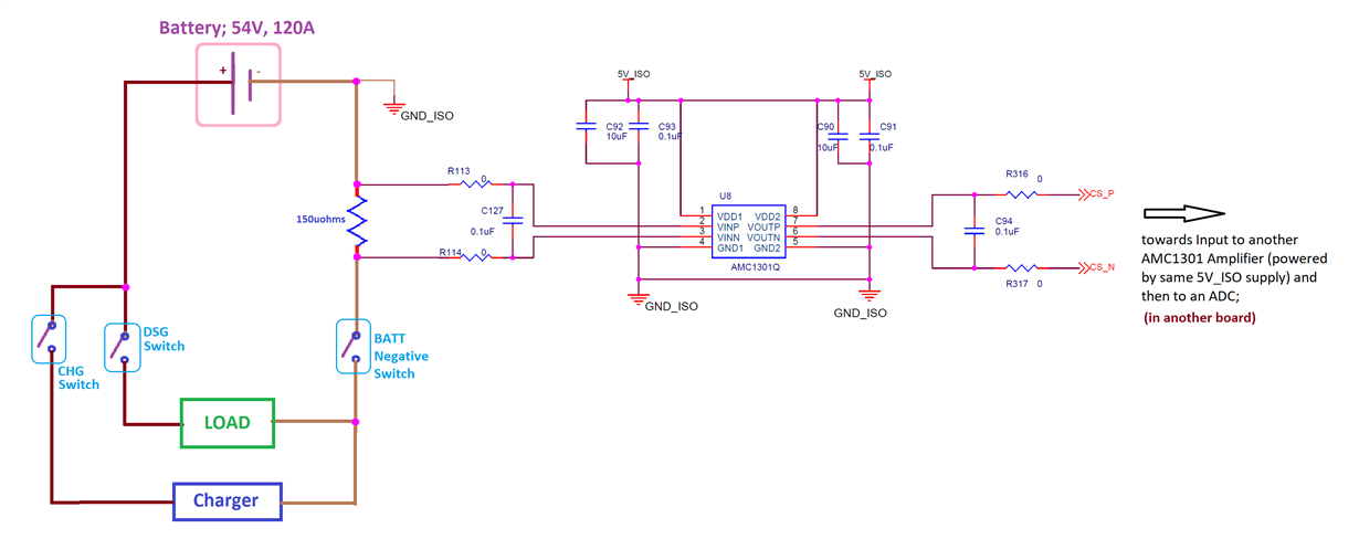
           We are using a Low side current sensing with Shunt resistor and AMC1301 amplifier as shown in the below circuit;

with this implementation in actual board, it is observed that the AMC1301 used in this circuit gets heated up and internal damage occurs (like sometimes internal short between Output side pins like VDD/Vout and GND occurs); 

Please help to let know if any issue in this implementation;

Note: Same Supply/GND used for both Input and Output sides; GND gets shorted to VinP;

Background: Reason for using the AMC1301 based isolation amplifier is that there are multiple same parts used for other isolated functions; hence used the same here for Diff to Diff amplifier requirement;

Thanks and Regards

  • Hi Rohith,

    This is certainly not normal behavior for the AMC1301 or any of our isolation devices. 

    Your schematic didn't come through, can you re-post it? 

    Using the same supply/GND for both the input and outputs defeats the purpose of the isolation amplifier, which is to provide isolation from the input to the output side. 

  • Hi,

           Thanks for your response.

    Please find the schematic below,

    Yes, in this location, AMC1301 is used in non-Isolated mode (as diff to diff amplifier);

            Please help confirm if any other issue in the functionality with this implementation;

    Thanks and Regards

  • Hi Rohith,

    There is no non-isolated mode for the AMC1301. 

    Furthermore, either VINN or VINP should be connected to GND1. In your case, I would suggest connecting VINP to GND_ISO in order to ensure that the measurement stays within the common-mode input range.

    I also see in your diagram that the output of this AMC1301 goes to another AMC1301 on the same power supply. The output of this first AMC1301 will be on a common-mode output voltage of 1.44V and will most certainly not be within the input range of the next AMC1301 if they are using the same power supply. 

    Instead of using the AMC1301 in this manor, I would suggest using a typical operational amplifier. 

    Looking at the shunt resistor, 120A * 150uohm is only 18mV, so I understand your need for additional amplification. Instead of using the AMC1301, you could use the AMC1302 which has an input voltage range of +/-50mV instead of +/-250mV. From here, you could consider slightly increasing the size of the shunt resistor depending on your accuracy requirements. 

    How are you generating the power supply being used in your circuit? 

    Another device to consider is the AMC3301, which is the same as the AMC1301, however it has it's own integrated DC/DC converter. 

  • Hi Alexander,

    Thanks for your timely response,

    Regarding the VCM range of the second AMC1301 in the next board;

    As per datasheet specification, the Specified common-mode input voltage = VDD1 – 2.1 (max) [ Here: 5-2.1= 2.9V]. Hence the output VCM of 1st AMC1301 (1.44V) is within the input range of the second AMC1301.  (Both differential and Common Mode voltage) ( eg: 18mV * 8.2 = 147.6mV diff input to second AMC1301 which is well within range of +/- 250mV)

    I accept your suggestions on alternate implementation modes, and will do so if necessary,  we can plan for part change in the same board using AMC1302;

    but, currently, please help to confirm the circuit correctness of the of current implementation as we are observing higher stress and part damage in this implementation.

    The 5V_ISO power is already derived from a 5V supply available on board; used for sourcing multiple loads within the same Isolated domain;

    Thanks and Regards

  • Hi Rohith,

    There is no non-isolated mode for the AMC1301. Tying both grounds together is not recommended operation of the device. 

    VINN or VINP should be connected to GND1. In your case, I would suggest connecting VINP to GND_ISO in order to ensure that the measurement stays within the common-mode input range.

    For the anti-aliasing filter R113, R114, and C127 we recommend using 10ohm, 10ohm, and 8.2nF, yielding a cutoff frequency of ~1MHz. 

  • Thanks for your support.


    Yes, currently, the VinP is connected to GND_ISO in the board (using 0-ohms R113);


    Regarding the part usage in the given low side current-sense circuit;

    • is there any issue in using the AMC1301 with same GND and Supply rail on both Input and Output sides;
    • like any damage/degradation possible to the IC itself or its function of current sense amplification;
    • is there any minimum difference in Supply voltage expected between both the isolated Input (VDD1) and Output (VDD2) sides;


    Also, if possible, please help let know if any non-isolated part available in TI nearly matching the Footprints/pinouts of AMC1301 (differential to differential or single to diff);

    • to replace in board if required; in case any issue in the current implementation;

  • Hi Rohith,

    Theoretically, there should be no problem using the same supply and GND connection for both sides. No damage or error should occur and no minimum difference in supply voltage expected between the two. 

    I am not aware of any similar devices in terms of footprint and functionality that are non-isolated. 

    What types of switching are you using for DSG, CSG, and BATT? Can you share any waveforms that show their behavior? It is possible that transients from these switches are damaging the low-side of the part.