This thread has been locked.

If you have a related question, please click the "Ask a related question" button in the top right corner. The newly created question will be automatically linked to this question.

OPA2210: Paralleling Operational Amplifiers in Transimpedance Configuration

Part Number: OPA2210
Other Parts Discussed in Thread: OPA657, OPA828, OPA192, OPA4192, , OPA211

Hi,

For achieving better voltage noise, one can connect amplifiers in parallel if the input noise current times the source resistance is several times lower than the input voltage noise.

With amplifiers intended for voltage gain this is not a big deal, as one can just build two or more identical amplifiers, connect their inputs directly and connect their outputs to the common output via identical resistors, which do the job of averaging the two or more amplifier outputs and limiting the current flowing between the amplifier outputs caused by different offset voltages.
Because the amplifiers only share one input terminal, their second input terminals can settle to different voltages, so the output offset between the amplifiers is usually just the input offset voltage times the voltage gain.

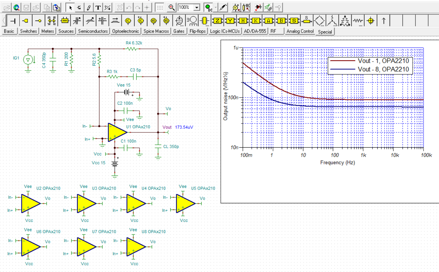
Now with a transimpedance amplifier configuration all the amplifiers would share both input terminals, which would result in bot outputs going to the opposite rails unless the input offset voltages were exactly the same.

Is there a good way to realize paralleling of amplifiers in the transimpedance configuration? I thought about zeroing the output difference with a slow servo loop offsetting the non inverting input of one of the amplifiers, but as my signal frequencies can be very low, the loop would have to be a very very slow one.

Thanks for any input.

Regards,
Gerd

  • Hi Gerd,

    even if you could build such a paralleled transimpedance amplifier, you would not have a benefit, because only a fraction of input signal current would flow through each individual transimpedance amplifier then. So after adding the signals from the individual transimpedance amplifiers you would end up with the same signal but with the increased noise coming from all the individual transimpedance amplifiers.

    And how to divide the input signal current equally between the individual transimpedance amplifiers?

    There are other techniques to reduce the noise of a transimpedance amplifier. One method to increase the signal-to-noise ratio is to increase the feedback resistor, as explained here:

    Another method is to use a JFET to bootstrap the cathode of photodiode (if is one used in your application). It eliminates the effect of photodiode capacitance. The positive effect is also discussed in the link above.

    Kai

  • The more direct way to get lower voltage noise for a transimpedance amp is to use a decompensated op amp, hence, parts like the OPA657 exist. 

  • Hi Michael,

    yes, of course, that's the most obvious thing to do :-)

    Kai

  • Hello Gert,

    And there is another reason why its is best not to connect the input and output pins of multiple op amps together. See the first part of Bruce Trump's blog from a few years ago:

    https://e2e.ti.com/blogs_/archives/b/thesignal/archive/2013/03/26/paralleling-op-amps-is-it-possible

    I am with Michael and Kai, apply the OPA657 if you are looking for a low noise, wide bandwidth +/-5 V supply solution. If you don't need quite as much bandwidth, but low noise and a +/-15 V supply solution consider the OPA828:

    https://www.ti.com/lit/ds/symlink/opa828.pdf

    Regards, Thomas

    Precision Amplifiers Applications Engineering

  • Hi,

    The amplifier would be in a transimpedance configuration, but the source does not have a high impedance like with photo diodes acting as a current source. The source impedance is about 200 ohms with about 1nF in parallel.

    I have to keep the voltage very low in order to avoid distortion (the current from the source is linear but only within a small compliance voltage range).
    So I cannot use a voltage gain amplifier, but I have to use a C-V converter like a transimpedance amplifier.

    Because of the low impedance also a low voltage noise is important and increasing RF above some value doesn't decrease the noise anymore. And I need it down to 1 Hz, so those wideband amplifiers are too noisy.

    In the last comment below Bruce Trump's blog, Neil Albaugh mentions that paralleling amplifiers indeed can reduce the noise.

    But it does not when connected like in fig. 1b. Fig. 1a would be OK if A2 would have gotten it's own feedback divider. Only in my situation there is no feedback divider but only a feedback resistor...

    Regards,
    Gerd

  • Hi Gert,

    I had the privilege of working with Neil, Bruce and Michael for many years. They really know analog!

    I am not opposed to the idea of using the parallel op amp architecture to reduce the noise. There have been plenty of implementations using various audio op amps across the years. My thought is thought is if you do try it that you use op amps that have very low voltage offset to avoid the issue that Bruce mentioned, and ones that have very low noise as well. Often, op amps designated for low-noise audio applications indeed have very low noise, but a dc parameter such as voltage offset is not as low as what you can have with an op amp slated for precision, industrial applications.

    The newer e-trim CMOS op amps may provide a good compromise between extremely low voltage offset and very low noise. The OPA192 is rated for a typical voltage offset of +/- 5 uV typical, and +/-25 uV max at room temperature. Its typical input voltage noise density voltage is 10.5 nV/√Hz at 100 Hz, and 5.5 nV/√Hz at 1 kHz. You can view the datasheet here:

    https://www.ti.com/lit/ds/symlink/opa192.pdf

    The OPA192 is available as a quad, OPA4192. If you decided to use 8 op amps in parallel, then it would require just two packaged devices.

    Regards, Thomas

    Precision Amplifiers Applications Engineering

  • Hi,

    I think the actual op amp is not the problem. The OPA2210 that I mentioned in the original post also has 5µV offset (35µV max).

    The problem is that due to the nature of the transimpedance amplifier the inverting input is a virtual ground. So a second op amp connected there would have an infinite non inverting gain (rFB/0).
    Actually this is also valid for any voltage noise, so my aforementioned idea of zeroing the offset voltage with a slow servo loop that offsets the non inverting input would only get rid of the problem with regard to the offset voltage (and maybe some very low frequency noise), but the voltage noise above the cut off frequency of that slow servo loop would still be amplified with infinite gain and completely saturate the op amp.

    Of course op amp number one would face the same problem as op amp number two would also introduce a virtual ground at its inverting input, making the non inverting gain of op amp 1 infinite.

    I could prevent this to some extent if I would not connect the op amps as transimpedance amplifiers but as inverting amplifiers before connecting them in parallel. Like inserting a 2 ohm resistor between the signal source and the inverting input.

    If the feedback resistor would be 20k this would result in a non inverting gain of 5026 for each of the two op amps (the resistance to ground from the inverting input would be the above 2 ohm in series with the parallel connection of the 200 ohm source resistance and the 2 ohm connected to the inverting input of the other op amp being a virtual ground).
    Because both op amp outputs are averaged in the end, the actual noise gain would be 2513.

    Wait. If op amp one has voltage noise, which is amplified by 5026 at its output, this voltage noise appears at its inverting input because the non inverting input is grounded. But the inverting input of op amp one is connected to the inverting input of op amp two via both 2 ohm resistors while there is still the 200 ohm source resistance to ground connected between them. So 0.99 times the noise voltage of op amp one (voltage divider of 2 and 200 ohm) is fed to op amp 2 with an effective source resistance of 3.98 ohms, resulting in a negative gain of 5025 to the output of op amp 2.

    So the overall noise gain would be 0.5, while the noise and offset appearing at each op amp output would be about 5025 times the actual noise and offset voltage of the op amp. 35µV offset would mean 176 mV output offset, which would be tolerable with +-14.5V output voltage range. As the 35µV is also the maximum offset voltage matching, the influence of the second op amp does not have to be added. With a gain of 5025 the bandwidth would be about 3.6kHz resulting in 132nV rms wideband noise. Taking a crest factor of 10, that makes 1.3µV pp. Adding the 0.09µV pp of 0.1 to 10 Hz noise, the noise at each op amp output resulting from one op amp's voltage noise would be 7mV pp, even much less than the output offset.

    This is crazy. I have to simulate that.

    The downside of that approach would be that the input impedance of the combined amplifier would no longer be 0 ohms as with the transimpedance configuration, but 1 ohm. So I would have to check if this would be OK regarding the distortions.

    If the maximum pertubation of the individual op amp outputs is 183mV in the above example, the question is, if I can sacrifice about 1.8V of output voltage range. If yes, then I could use 0.2 ohm instead of 2 ohm and arrive at 0.1 ohm combined, being much closer to the ideal 0 ohm of the transimpedance configuration.

    Anyone still with me? If so, please raise your hand ;-)

    Regards,
    Gerd

  • Hi Gerd,

    can you post a schematic which shows what you plan to do?

    Kai

  • The right part is the amplifier and as the current noise times 200 is an order of magnitude less than the voltage noise paralleling could reduce overall noise, especially around 1Hz.

  • Hello Gerd,

    I took your basic OPA2210 TINA circuit and changed the input VCVS to an ac current source. Otherwise, the high voltage gain of the circuit caused the output to hit the rail. Then I ran an output noise simulation with one OPA2210, and a second with eight OPA2210 op amps wired directly in parallel. The noise sources in the simulation circuit are uncorrelated and as expected Neil's parallel op amp configuration results in an appreciable reduction in the output noise.

    Regards, Thomas

    Precision Amplifiers Applications Engineering

    OPA2210_Noise_eight_OPA.TSC

  • Hello Thomas,

    Yes, the output went into saturation because of the inout offset voltage of the amplifier.

    I took care of this by adding 5,00429uV DC to the voltage source controlling the VCCS (I think I could have modified the offset voltage in the OPA2210 model definition, but I just made a DC sweep and used the DC voltage where the op amp output was close to zero).

    Unfortunately the DC bias voltage of my VG1 source was not displayed in the schematic.

    I wonder how using an AC source prevented the op amps going into saturation, but it seems to have worked for your simulation.

    But wait. I did the above when I opened the feedback loop in order to measure the phase margin. With a closed loop, the input offset voltage of only one op amp should not saturate the output. Or was there a default 1V DC in the source you had used in the beginning?

    Anyway, so you can confirm that paralleling the op amps gives about a 2.5 fold noise reduction (in the flicker region, where the op amp noise greatly dominates the source resistor noise).

    Now the problem in real life is that I can neither AC couple the op amps (because I need the DC signal), nor can I set a DC offset to sub nanovolt precision individually for each of the paralleled op amps.
    You can simulate what happens in real world if you vary the input offset voltages of the 8 op amps individually.

    Regards,
    Gerd

  • Hello Thomas,

    Did anything else come to your mind on how one could use parallel op amps in this circuit if they have different input offset (and noise) voltages like in real life?

    Regards,
    Gerd
    P.S.:
    I might switch to the OPAx211 because of the higher bandwidth and a bit lower noise at 10Hz and above. But even though it has a higher noise current, overall noise could benefit from two of them in parallel.

  • Hi Gerd,

    what exactly is your frequency range of interest?

    Kai

  • Hi Kai,

    From 0.1Hz to 1MHz.

    100kHz to 1MHz is more of a nice-to-have and doesn't need to be absolutely flat.

    Also, while the noise spectral density from 0.1Hz to 1Hz should be good, the noise from 1Hz upwards is more important.

    Regards,
    Gerd 

  • Hello Gerd,

    The OPA211 provides the best combination of lowest noise and wide bandwidth of our Precision Amplifiers op amp product line. It is a bipolar input op amp and its input bias current is higher than what is obtained with a JFET, or CMOS, input op amp. The latter types of op amps are most often applied in transimpedance amplifier (TIA) applications because of their very low input bias current, and the extremely light load they present to the input current source. However, that doesn't mean that bipolar input op amps can't be used for the application provided their higher input current is taken into consideration, and the load it presents to the input current source. 

    You mentioned that the source impedance of your application is very low. If its output current is high relative to the OPA211 input current I think it will workout well in terms of a load on the source. Additionally, since the source impedance is low the OPA211 higher current noise which is higher compared to a JFET, or CMOS, input op amp should result in little additional noise voltage generation.

    The lowest noise, widest bandwidth precision JFET input op amp that we have is the OPA828. Its noise at 1 kHz is typically 4 nV/rtHz, with a 45 MHz gain-bandwidth. There is an interesting graph in the OPA828 datasheet comparing the OPA828 and OPA211 noise performance vs source impedance, in a unity gain buffer configuration. The JFET input OPA828 gives the bipolar input OPA211 a run for its money when the source impedance gets above a few kilohms.

    Regards, Thomas

    Precision Amplifiers Applications Engineering 

  • Hi Gerd,

    I think the OPA211 suggested by Thomas is an optimum solution.

    Maybe you can furtherly lower the noise a bit by using a composite design? I would give this circuit a try:

    Instead of the triple MAT-03, which is obsolete now, I would take two single MJE371 or another 3...4A Ic and 30...40V Uce small power PNP plastic transistor. These provide the lowest base resistances, important for lowest noise here. Buy some dozens of these transistors and hand select them for lowest noise. Also, play a bit with the collector current and supply voltage.

    Of course, some other designs could be checked as well. Here's a nice link:

    Uwe Beis is using an NPN design, though.

    Good luck :-)

    Kai