This thread has been locked.

If you have a related question, please click the "Ask a related question" button in the top right corner. The newly created question will be automatically linked to this question.

PGA281: How to have into account Digital threshold for control signals when VSON is negative

Part Number: PGA281
Other Parts Discussed in Thread: OPA2320

Hi guys, I'm Jose.

I want to use the PGA281. For VSOP = 2.5 V and VSON = -2.5V. When using a negative supply for VSON, the datasheets says "The negative digital supply is connected to the VSON pin. Take care if using split supplies on the VSOP and VSON pin because the logic low and high thresholds are determined by DVDD and VSON. In normal operation, VSON is connected to the system ground."

I've been seen a simulation which I downloaded from a link in the datasheet. Basically I modified it because all examples I found in the datasheet are specified for VSON=GND.

So, I want to know what would be the digital thresholds when using a VSON=-2.5. In the simulation I have:

VSOP=2.5 and VSON=-2.5

VOCM = 0V

INP = sine signal of 500mV and 100kHz

INN = sine signal of -500mV and 100kHz

GAIN = 1

DVDD= 2.5V ( As DVDD-VSON = 5   is correct because 2.7<5 <5.5 as per the datasheet indication). 

Thank you, I hope someone can explain this to me, and get the correct simulation.

PGA281RTDFig52.TSC

  • Sorry, I forgot some of the units. everything is in Volts [V]

  • Hi Jose,

    Yes, the PGA281 will support VSOP=+2.5V and VSON=-2.5V with VOCM=0V, and DVDD=+2.5V.  As you have correctly mentioned, the digital supply levels need to be referred to VSON=-2.5V, and you will need to level shift the signals and refer them to the VSON=-2.5V and DVDD=2.5V.

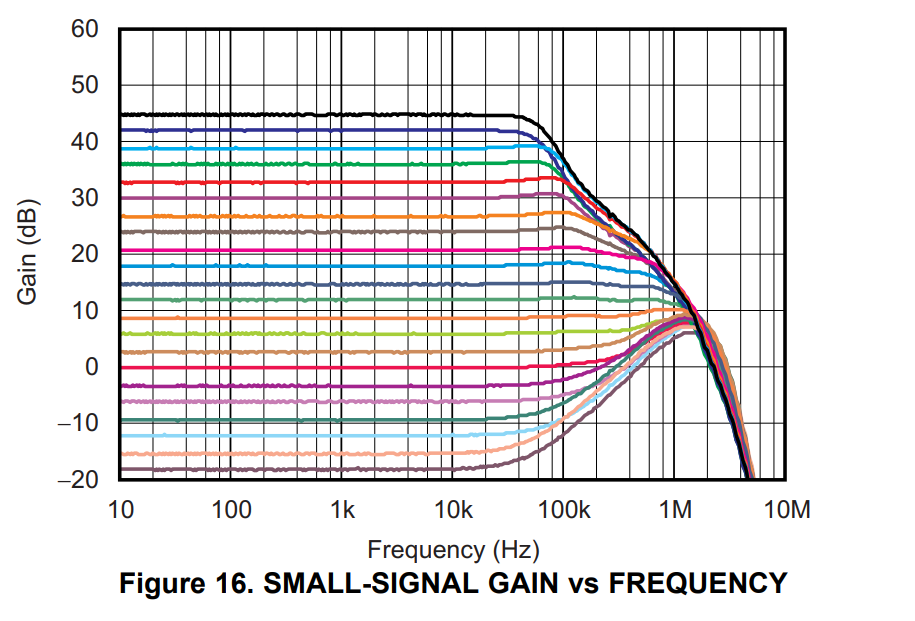
    Does your application require to support input signals with frequencies around 100-kHz?  The PGA281 is an instrumentation amplifier optimized and intended for high DC precision applications supporting relatively low bandwidth signals.  The small signal bandwidth vs gain is shown on page 9, Figure 16.  At frequencies above 10 or ~20-KHz, the small signal gain (or attenuation) is no longer constant and starts to decrease with frequency.  The device will not offer good results at frequencies above ~20kHz (will not work at 100-kHz) as the gain (or attenuation) decreases with frequency; and 100kHz signals are outside the PGA281 bandwidth.  Please see below.

    If your application only requires input signals of 10kHz or below, we could look into a voltage level translator to support the gain control signals...  Are you planning to use a microcontroller to configure the PGA281 gain interactively?  If yes, please let me know the digital supply voltage level for the micro-controller you would like to use and we could look for a voltage level translator. 

    PS. The TINA macro-model has a limitation and does not support the PGA281 when configured with VSOP=+2.5V and VSON=-2.5 at this point in time; however, the device does support this mode of operation.

    Thank you and Regards,

    Luis

  • Hi Luis, 

    Thank you for answer. Well, this forum with your answer has been very useful, in the first place I had not analyzed  yet that graphic about the behavior at different frequencies, so thank you so much for this great reminder. I wanted to use this  PGA281 for an ADC which can work at 1MSPS (500kHz max signal) and other that work at 125kSPS (~62.5k max signal), but with that you have told me this IC would not work at such frequencies. But, I think that at the end the sample rate I'll define would be around the ~20kHz (so ~10kHz max) so having it in the correct range for this  PGA281.

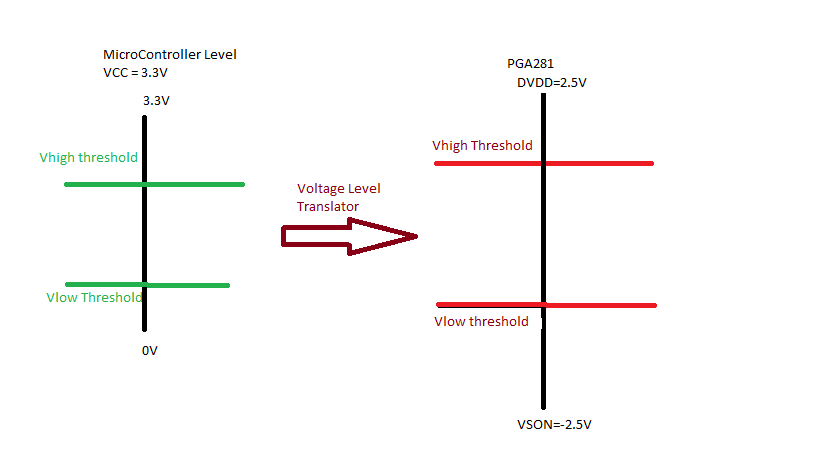
    Regarding the interactive gain, yes, I plan to use a microcontroller which would be at 3.3V. Thank you, I'd like to know which voltage level translator would be used. With this what I understand, would be to translate as shown in fig.1 (attached), from a scale of 0V-3.3V to a scale -2.5 to 2.5V, is that correct? 

    But here I'm a bit confused. would you explain me what would be the specific range values for  Vhigh and Vlow levels in the scale of -2.5V to 2.5V?

    I also would like to ask you, how did you know about this "The TINA macro-model has a limitation and does not support the PGA281 when configured with VSOP=+2.5V and VSON=-2.5"?

    Luis, Thank you so much for your help.

    Fig.1 Voltage level translator

  • Sorry, the figure was not attached correctly in my answer

  • HI Jose,

    The logic high level and low level thresholds are defined on the datasheet below; where "DVDD" represents the difference between DVDD-VSON; and the absolute voltage needs to referred to VSON:

    Therefore, for the case VSON=-2.5V, and DVDD=+2.5V, the max logic low threshold:  VIL(max)=-2.5 + 0.2(5V) or VIL(max) = -1.5V

    and the min logic high threshold:  VIH (min) =-2.5 + 0.8(5V) or VIH (min) = +1.5V

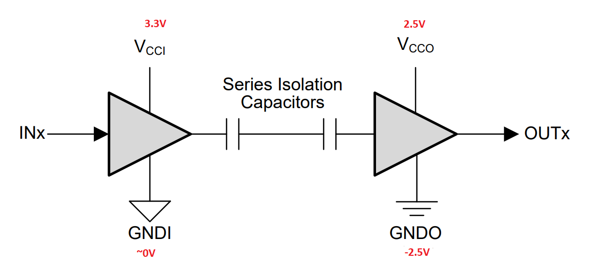
    Regarding the voltage level translator, one possibility is to use a digital isolator such as ISO776x (or other similar solution)   

    When VSON is set to a negative voltage, the TINA macro does not model properly (the different gains do not scale properly).  There is a request with the modeling team in the queue; however, this is an older macro, and there may be challenges accessing or modifying the original source files. 

    As a temporary solution, attached is a simulation where I used a VCVS to shift the output voltage signal to VOCM=0V, using the existing PGA281 model.  This is only to help you visualize the output signal shifted to VOCM=0V.

    sbom817_PGA281_modified.TSC

    If you intend to drive a SAR ADC at high sampling rates, this depends on specific the sample-and-hold structure of the ADC, you may consider placing a relatively high bandwidth dual amplifier buffer (one amplifier at each output) or a FDA at the outputs of the PGA281 prior the ADC.  SAR ADCs (and some Delta-Sigma converters that do not incorporate a buffer) present a dynamic load impedance and require a relatively high bandwidth (low output impedance) amplifier driver. 

    The PGA281 may not have enough bandwidth (or low output impedance over frequency) to drive a SAR ADC, unless you use a very slow sampling rate (<30-kSPS).  One possible dual buffer amplifier could be the OPA2320 (20-MHz dual amplifier).

    Thanks and Regards, 

     Luis

  • Hi Luis,

    Thank you for your useful explanation and for the file attached.

    Regarding the level translation with a digital isolator, for example ISO7761, I think this would be something like the figure below, i.e, VCCI=3.3V GNDI=0V  and VCCO=2.5V and GNDO=-2.5V, with this the logic values for PGA281 will be correct. Is it correct the interpretation for the digital isolator?

    Thank you 

    Regards

    Jose

  • Hi Jose,

    This is correct.

    Thank you and Regards,

    Luis

  • Thank you, Luis. I appreciate your help with this.