This thread has been locked.

If you have a related question, please click the "Ask a related question" button in the top right corner. The newly created question will be automatically linked to this question.

INA2181: Please review and simulate the schematic for development

Part Number: INA2181
Other Parts Discussed in Thread: INA2290, INA181

Hi E2E Team,

my customer designed schematic with INA2181, they want to verify and  simulate it.

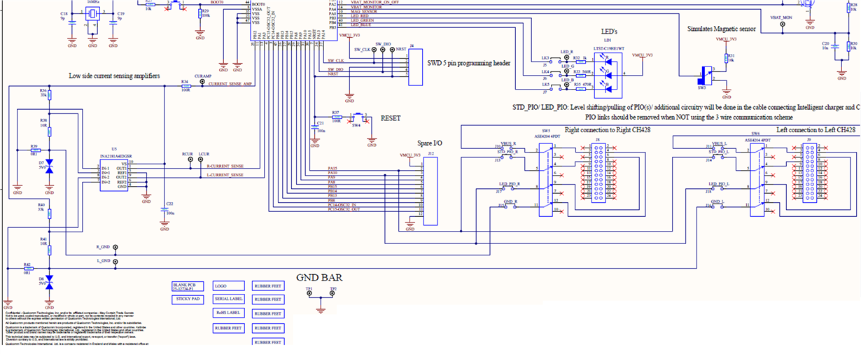
the schematic is below;

the results in customer was;

1mA input in INA2181 => 200mV output

6.5mA input in INA2181 => 400mV output

Please check this issue. Thanks.

Best regards,

Chase

  • Hello Chase,

    Thanks for considering to use Texas Instruments.  In Ideal world your customer should get an output of Load*Rshunt*gain.  Based on your schematic I would therefore expect 1mA*10Ω*200V/V=2V and 6.5mA*10Ω*200=13V.  However, the device has limitations and inherent sources of error. Since the INA2181 supply comes from what looks like a microcontroller, I presume it to be around 3.3V. The output that should go to 13V will rail somewhere beneath that.  As for the 1mA measurement you will likely see a large error due to input offset, which is influenced by the supply, common mode, and input bias currents.  As your customer's configuration is a low-side setup, I do not expect much influence from input bias currents.  However, the common mode and supply can have a significant contribution.  I use the max spec values adjusted according to the conditions I see along with our RSS formula, your error could be as high as 7.8%.  We have alternative parts with lower Vos and higher CMRR specs which would better address this range, but they are more expensive and typically 1 channel.  The INA2290 is the only 2 channel device that should have lower error. 

  • Hello Patrick,

    Thank you for your reply. Actually I did not understand some of your saying, I just saw that there are some error and unclear thing on our conditions.

    there is some new test conditions;

    1. on the end of R_GND and L_GND, there are the wireless earbuds each, they attach J8 and J9 connector.

    2. pin4 of J8 and J9, are connected to earbud's of GND, and also connected to R_GND & L_GND.

    3. pin3 of J8 and J9, are connected to VBUS(5V) which charges the battery of earbuds typically.

    4. when the earbuds want to communicate with MCU, they temporarily stop charging, and control the current in 2 ways, 1mA and 6.5mA. this means 0 and 1 as binary scale.

    5. of course these current values are sent to IN2181, through R38 and R39.

    6. and finally IN2181's outputs are in 2 types, 200mV in 1mA situation, and 400mV in 6.5mA situation. the MCU accept this, and convert it to 0 and 1 as binary scale.

    they say that there is no other option because PCB size is very very small, they did not have much space to design more ICs to communicate the earbuds and MCU.

    and finally they designed the way, which the earbuds send the signal as current, and the MCU receive the signal as voltage. and there is IN2181 between current input and voltage output.

    anyway i think there is the key that the change of current by earbuds affects to the sensing current for INA2181. unfortunately i don't have any more idea.

    what i want to know is, is it okay to design the schematic like this for our purpose, and is it possible to simulate with PSpice or some other tools for the proof.

    please check this issue. Thanks.

    Best regards,

    Chase

  • Hello Chase,

    In your or your customer's schematic, they use the INA2181A4.  A4 corresponds to the 200V/V gain variant of the INA2181. The sense resistors R38 and R41 are labeled 10R, which I interpret at 10Ω, while R39 and R42 are labeled 0R1, which I presume are either 0Ω or 100mΩ and therefore comparatively negligible.  Our device output is Load (A)*Sense Resistance(Ω)*INA2181 Gain(V/V) + REF(V).  That is how I got 2V and 13V.  However, 13V output is not possible because the INA2181 cannot exceed its supply, which at most is 5.5V and most likely less than that because the INA2181 supply looks to be sourced from the microcontroller.

    If your customer changes the INA2181A4 to INA2181A1, then for 1mA and 6.5mA across either R38 or R40 they will get an output of 200mV and 1.3V. You can verify this with either pspice or TINA. We have relevant models for both simulators available on the product page under Design Tools and simulation.  While the available models are only the 1 channel version of the device (INA181), you can still expect the behavior to be the same to a given channel of the INA2181.