This thread has been locked.

If you have a related question, please click the "Ask a related question" button in the top right corner. The newly created question will be automatically linked to this question.

LMH730316: Gerbers and Performance

Part Number: LMH730316
Other Parts Discussed in Thread: LMH730216, , DUAL-DIYAMP-EVM

We are designing an instrumentation amplifier based on the LHM6703 SOT-23-6.  There was a previous request for the LMH730316 gerber files. TI replied that they didn't have the gerber files for the LMH730316 and recommended the LMH730216.  Was this only because the LMH730216 gerbers are available or is the high-speed performance of the LMH730216 better than the LMH730316.

I there a high-speed instrumentation amplifier circuit evaluation board based on three discrete op-amps that is available from TI for reference?

Thank you!

  • Hello Andrew,

    Will look into the differences between LMH730316 & LMH730216

    In regards to your question about instrumentation amp board, the DUAL-DIYAMP-EVM features a two amp instrumentation configuration & a difference amp configuration that you can use. Note, however, these boards aren't designed with high-speed circuits in mind.

    Best,

    Hasan Babiker

  • Hello Andrew,

    These two boards should offer similar high-speed performance, although we only have gerbers for the LMH730216 boards.

    Best,

    Hasan Babiker

  • Hasan,

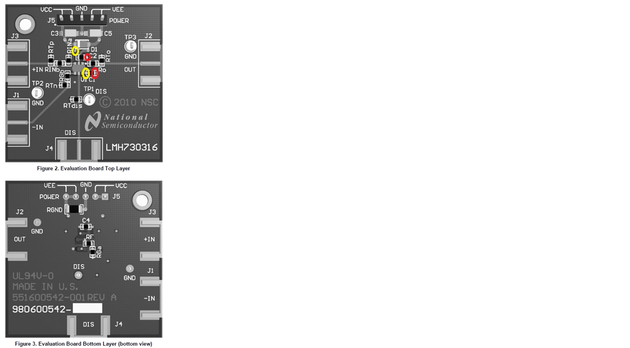
    Since you don't have the gerbers, would it be possible to post a picture of the bottom of the board?  The grayscale image in the User Guide for the board makes it hard to tell exactly where the metal is cleared on the bottom layer.  An image of the top of the board is on the product page.  I think boards are two weeks out.

    Thanks,

    Andrew

  • Hello Andrew,

    Unfortunately we don't have any additional photos for the bottom of the board.

    Best,

    Hasan Babiker

  • Hasan,

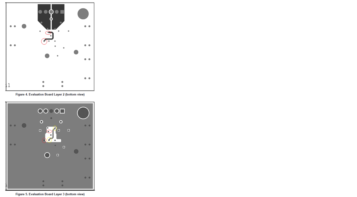
    There is a ground trace on Layer 2 shown below.  I believe this trace connects the GND pads of C1 and C2.

    I believe this trace taps the edge of the GND plane on Layer 3 at the via the is in the GND pad of C1.


    I believe the GND trace on layer 2 is providing isolation between the +IN (pin3) and OUT (pin1) as well as isolation between -IN (pin4) and OUT (pin1) of the opamp while minimizing the parasitic and stray capacitance.  I was surprised that the GND pad of C2 did not tap off of the solid ground plane on Layer3.  Was this because the a ground loop would have existed?  Any insight you can provide would be greatly appreciated.  I believe the GND trace on Layer2 is red and the trace on Layer3 is the +VS in yellow.

    Thanks,

    Andrew

  • Hello Andrew,

    It looks like your images didn't go through. Would you mind posting again and using the "Insert /Edit Media" button for uploading images?

    Best,

    Hasan Babiker

  • Hello Andrew,

    Thanks for reuploading the images. I agree with the statements you made and that the vias correspond to GND and +VS. 

    In regards to the GND via of C2 it's not clear to me why it was done in this way. It seems to make sense to tap to the GND layer that is only slightly further to the right (from top view perspective). I've also consulted one of our layout experts and their observation was that adding the trace in the second layer appears to only increase the inductance between C2 and GND.

    Best,

    Hasan Babiker