This thread has been locked.

If you have a related question, please click the "Ask a related question" button in the top right corner. The newly created question will be automatically linked to this question.

LPV521: Voltage Controlled Current Sink

Part Number: LPV521

Hey team,

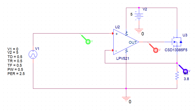
Just wanted to run some simulations by you for a voltage controlled current sink design. I had one odd measurement that I was curious to get your thoughts on. Attached is the schematic and graph in question.

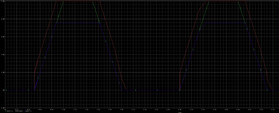
The red line above shows the voltage at the gate (output of the amplifier), the blue line is the output voltage at the source (negative terminal of the amplifier), and the green line is the input voltage.

The area I'm curious about is the output of the amplifier being around 1.2V higher than the input towards the start of the simulation. My assumption would be it has to do with negative feedback, but the graph doesn't look like how I would imagine it to be. I would expect the voltage over the negative terminal to be 0V until Vgs (or Vthreshold) is hit from the nFET (which is 1.2V maximum).

I'm sure I'm just missing something fundamental here so I appreciate the help! I'm aware that my design could likely be improved by adding a voltage divider at the input to pull the 5V down lower so that the tracking extends from 0-5V rather than 0-3.8V.

Cheers,

Cameron

  • Cameron,

    The circuit tries to match blue to green so red has to be VGS higher.


  • Yeah that is of course the goal of the amplifier. I guess what really generated my question is that I'm not used to seeing such a steep curve to hit that tracking goal. It just feels odd that when I input less than Vgs to the amplifier the negative feedback will actually help drive a +Vgs on the output.

  • Cameron,

    The DC gain of the op amp is typically 1,000,000 (120dB).  Putting the op am in a unity gain loop makes the forward signal gain 1. However the op amp gain is still 1,000,000. The op amp in unity gain setup uses all of the seeming extra gain to reduce the input error to a tiny level that happens to be the op amp own offset error, Vos. Basically Vos is the op amp idea of what zero input means. For no or an attempt for negative FET current, the output should be zero (VOL) limitation of op amp where gain will hit zero. For a small FET current the output has to be at VGS, say 1.2V and the op amp has a 1 million gain so the first 1.2uV of input (beyond the Vos error) will make that happen. 

    If the Vos of the amp amp was say +300uV, then a 0mV input would have a output at VGS level and output current would be 300uV/3.8 ohm.  In other words, not off.