This thread has been locked.

If you have a related question, please click the "Ask a related question" button in the top right corner. The newly created question will be automatically linked to this question.

PGA281: Connect an ADS8900 to an PGA281

Part Number: PGA281
Other Parts Discussed in Thread: OPA625, ADS8900B, THS4031, OPA2320, OPA320

Hi, 

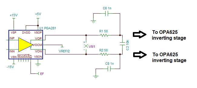
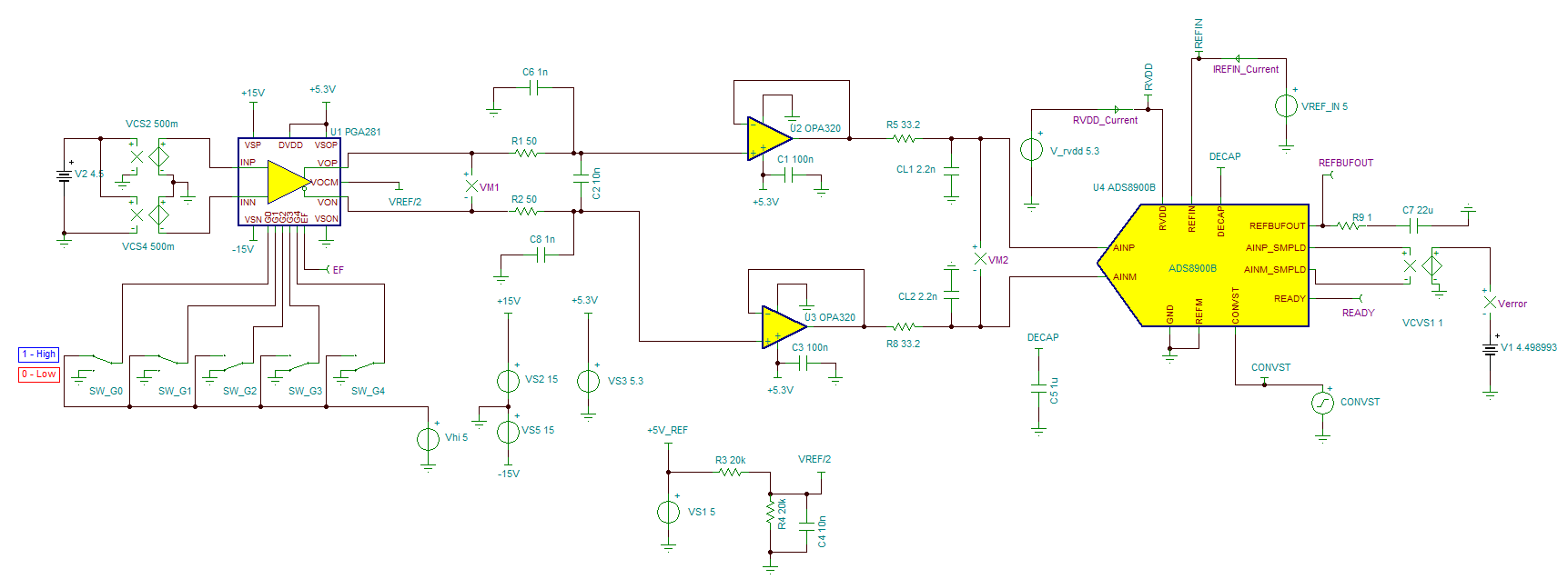
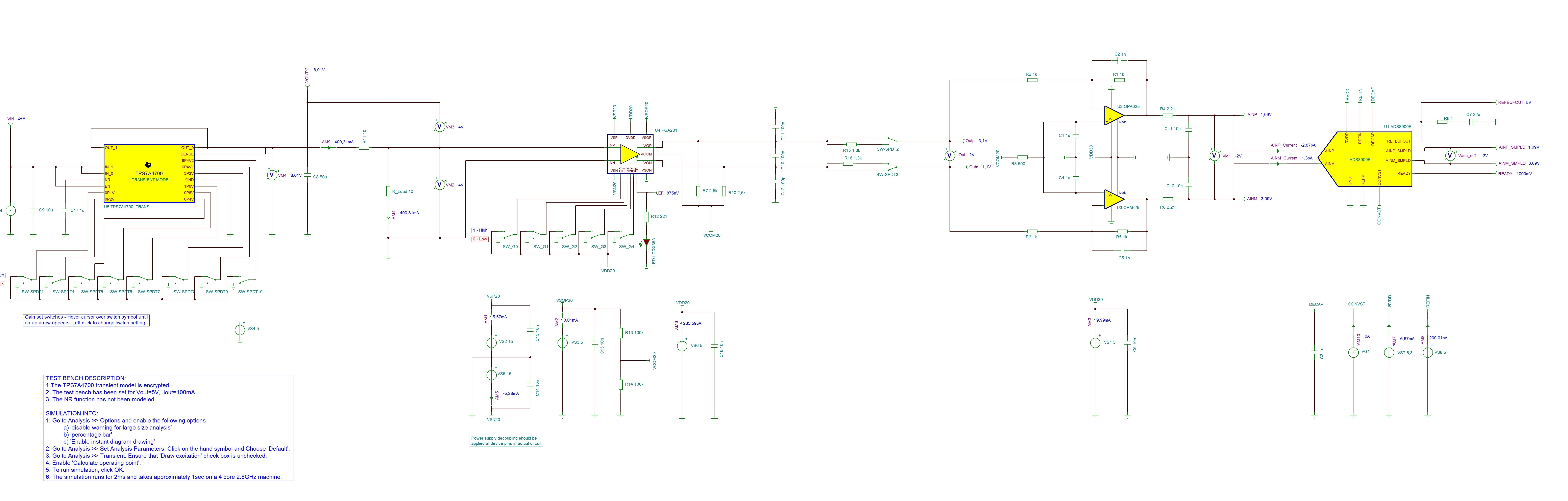
I'm looking for an PGA, so that I can measure a voltage level from 0,01V to 10V with an ADS8900 SAR ADC.

Can I connect the ADS8900 with one of these circuits to the PGA281?

or

Thank you very much

Best regards

Patrick

  • Hello Patrick,

    The solution on top with the PGA281 buffered with the OPA625 in the inverting configuration could work. However, please place an R-C-R filter between the PGA281 and OPA625 inverting stage of 50-Ohm-10nF-50ohms and 1nF common-mode filters as shown below.  This is to reduce any low level residual chopper noise from the PGA281.

    The THS4031 proposal at the bottom does not have the proper RC filter between the ADS8900B, and THS4031.  There is also a potential risk that the THS4031 (powered by higher voltage supplies than +5.3V) can expose the ADS8900B to over voltage during a fault or power-up/brown out condition. 

    An alternative solution is to use instead the dual OPA2320 in buffer configuration (non-inverting) powered with the 5.3 RVDD supply as shown below.  The RC filters (33.2-Ohm and 2.2nF) between the OPAx320 and ADS8900B have been tuned for proper OPAx320 and ADS8900B sample-and-hold settling response.  I also placed the R-C-R filter between the PGA281 and opa2320 buffer stage: 50-Ohm-10nF-50 ohms and 1nF common-mode filters as shown below.  

    Please let me know if you have any questions,

    Thank you,

    Kind Regards,

    Luis

  • Hello Luis,

    thank you very much for the information and the alternative solution.

    There for one more question. Is it better to use one OPA2320 or two OPA320?

    Attached could be find the new Ti-TINA simulation modell.

    ADC-V3.0.TSC

    Thank you very much

    Best regardsatrick

  • Hi Patrick,

    The design looks great, please only adjust slightly the RVDD supply (ADS8900B analog supply) from +5.2V to +5.3V. Since the ADC device is using a reference of VREF=+5V, the minimum ADS8900B RVDD supply required is +5.3V.  Also, I am assuming that you are using the 100kOhm-100kOhm voltage divider on the +5V reference to generate the VOCM bias voltage.

    You could use the dual OPA2320 for the buffer.  This will save you PCB board layout space.  Performance when using two singles or a dual op-amp is virtually the same, perhaps the dual offers slightly better matching in offset drift, but the performance in essence will be about the same when using  a dual or two single op-amps.

    Thank you and Regards,

    Luis


  • Hello Luis,

    thank you very much for the informations.

    I will finish the design next week, but on the PCB it would look like this.

    Thank you very much

    Best regards

    Patrick

  • HI Patrick,

    The image above does not display properly, but I will be happy to review your board layout,

    I will also share via email later today a layout example of a similar design of the PGA281, OPA2320 and ADS8900B.

    Thank you and Regards,

    Luis

  • Hi Luis,

    thank you very much for your help and a layout example.

    Attached you can find my picture from my last post.

    Thank you very much

    Best regards

    Patrick

  • Hi Patrick,

    I have sent the board layout design files for the PGA281+OPA2320+ADS8900B board via email.

    Many Thanks,

    Kind Regards,

    Luis