A related question is a question created from another question. When the related question is created, it will be automatically linked to the original question.
If you have a related question, please click the "Ask a related question" button in the top right corner. The newly created question will be automatically linked to this question.
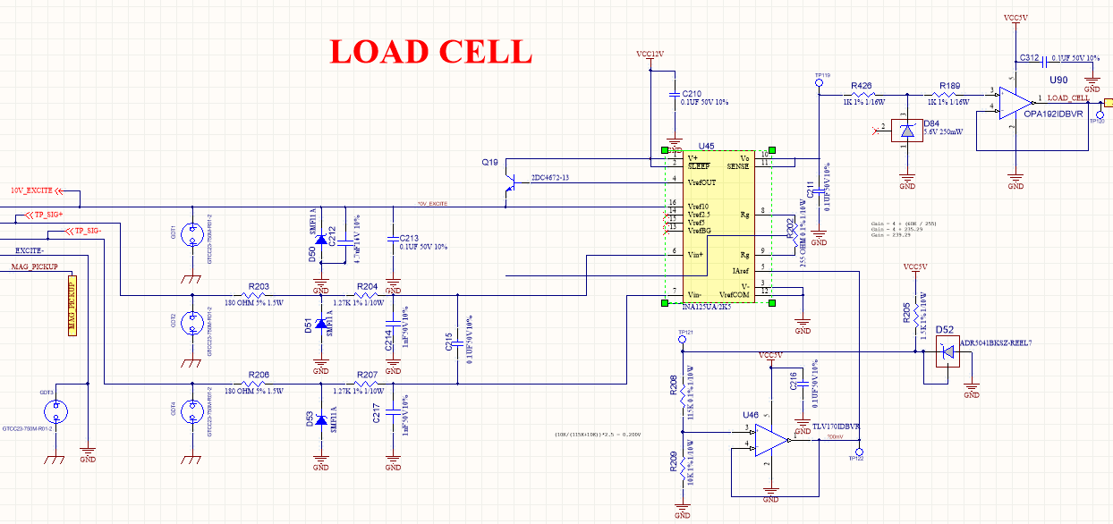
I will comment on the input sections after I have more information. I am not sure that D84 is needed. The output Vout = (Vin+ - Vin-)Gain + Vref. I am not sure that the purpose to clamp the output at 5.6Vdc. You have already implemented the voltage clamp at the input of the INA125. The OPA192 buffer is only allowed to operate within 5Vdc because of its common mode voltage requirements.
Based on your schematic, the max. differential input voltage is approx. (5V-0.4V)/239.29=19.2mV. You have LPF (RC) with cutoff frequency at approx. 125Hz. I would place the filters at the front of wheatstone bridge, including clamps and gas discharge tube etc. to minimize the input errors from the differential measurements.
I just know that the output of load cell is 2mV/V +/- 0.3V. I dont know any other information about the input being given.
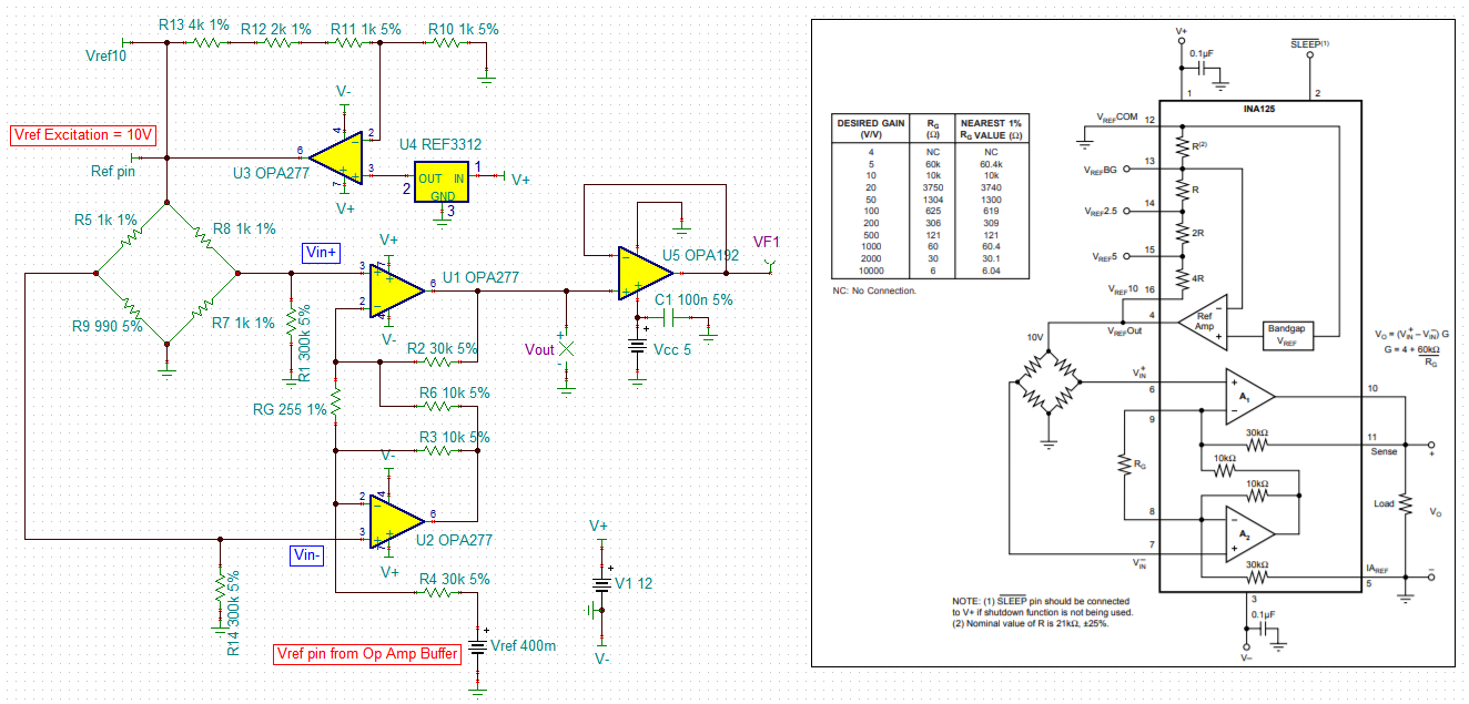
Also I have used IAref = 200mV. I think you have considered 400mV as IAref in your calculation.
OPA192 is only used for buffering the output of INA125. D84 is used just in case if any high voltage occurs to protect the opamp. The minimum breakdown voltage is 5V and max breakdown voltage is 5.6V for D84.
I just know that the output of load cell is 2mV/V +/- 0.3V. I dont know any other information about the input being given.
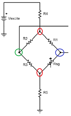
If the strain gauge has 2mV/V output signal, it means that with 10V excitation voltage applied to the wheatstone bridge, it will generate 2mV/V*10V=20mV at the full range or full scale (FS). I think that +/-0.3V may be a typo. Should it be +/-0.3mV? The strain gauge under the applied 10V excitation voltage is 20mV (FS) +/-0.3V will not make sense.
From the information you provide today, INA125's gain is too high. From the previous reply, the input of INA125 is approx. 19.2mV in FS. INA125 will operate ok, but OPA192 buffer will be saturated, unless your application is working under FS load. There should be another piece of information about the FS, which it should represent weight, pressure or force etc. that is proportional to the FS of output load cell (you will need the information). Also, please find the datasheet for the transducer, if you can.
If you have the load cell, please measure dc resistance between red-red circled node, red to green and green-blue circled nodes. From the measurements, you are able to calculate R1, R2, R3 and Rstraingauge. R1=R2=R3 should be equal in this case.
Also I have used IAref = 200mV. I think you have considered 400mV as IAref in your calculation.
If the zener voltage is 2.5V, the 2.50V* 10k/(115k+10k) = 0.2V or 200mV. I assumed 5V when I made the calculation.
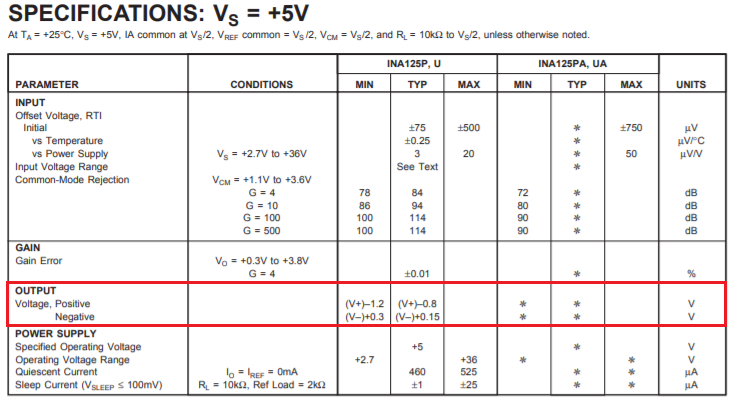
The transfer function of the INA125 is Vout = (Vin+ - Vin-)*Gain + Vref, where Vref = 200mV or IAref node. Below is output voltage range, which it indicates that Vout needs to be above 300mV when no load is applied (typical is (V-)+0.15V or 150mV in your case). You have Vs = 12V, but the this requirement should be similar.
Anyway, if you are able to provide me the data above, I should be able to simulate the configuration for you.