This thread has been locked.

If you have a related question, please click the "Ask a related question" button in the top right corner. The newly created question will be automatically linked to this question.

TL331-Q1: Questions from Application Report SNOAA35A

Part Number: TL331-Q1

Hello, Team,

The customer is considering to use TL331-Q1 and have 3 questions related to the Application Report (https://www.ti.com/lit/an/snoaa35a/snoaa35a.pdf).

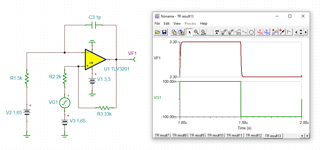
  1. It is stated in section 2.8 that in order to prevent oscillations and false-triggering, the output and input traces need to be kept separated when the source impedance is greater than 25kOhm.
    Is there any technical reason behind this "25kOhm" value? If so, could you please explain why it is "25kOhm"?
  2. After sorting out the layout, what kind of method can we use to evaluate a margin in terms of the oscillation?
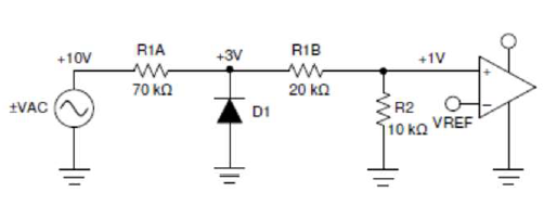
  3. In the circuit given in the section 2.9.2.1, the source seems to be divided into R1A (70kOhm) and R1B (20kOhm).
    Can this be regarded as the source being under "25kOhm"?

Thanks,

Masaru

  • Hi Masaru,

    the usual remedies are lowering the source impedances, adding filtering and hysteresis. Also the layout can be an issue, as discussed by Paul in the appnote. From my own experience oscillation is rarely problem unless fast comparators are used or comparators with very improper layout. But I do always add hysteresis!!

    Can you post a schematic? It's easier to discuss this issue with a concrete circuit :-)

    Kai

  • Hello, Kai,

    The schematic for 3 is below:

    (*from Application Report page 9)

    I think the questions are generic and independent of circuit design.

    Thanks and Regards,
    Masaru

  • Hello Masaru,

    The 25k was selected because a 50k + 50k divider string is common - and I did not want to cause panic in existing designs. The original datasheet said 10k. The lower the better.

    If it oscillates, that is a combination of input to output coupling due to layout, source impedance, input voltage differential, input edge rates, output voltage swing, reference bypassing, comparator supply bypassing and pull-up resistor supply bypassing. There is no particular formula, just common sense guidelines.

    A common cause is where large (>500k) reference divider resistors are used without a bypassing capacitor on the reference tap. This makes the reference voltage a high impedance node (250k), and also causes reference glitches due to changing bias currents and differential capacitance shoot-through at the input. The reference bypass capacitor lowers the AC impedance. Capacitors should NOT be placed on a positive node if hysteresis is used.

    The input impedance of the Figure 7 circuit is less than 10k since the 10k to GND dominates. Rsource = R2 // (R1A + R1B + Rsensor).

    To summarize; Oscillations tend to occur when the input signal is high impedance, the output has a large swing, and there is large capacitive coupling between the positive input trace and the output trace.

    Usually this is caused by running the input trace next to the output trace for a distance. This can create 10's of pF of coupling between the traces. The fast output edges shoot right though this capacitance. Just be sure there is a ground or guard between the input trace and the output. Do not run the input and output traces in parallel, always at right angles.


  • Hi Masaru,

    here some examples showing what can happen when improperly using a comparator:

    masaru_fast_comparator.TSC

    Kai

  • Hi, Kai,

    Thank you very much for providing detailed information!

    Best Regards,
    Masaru Oinaga

  • Hello, Paul,

    Thank you very much for your kind support.

    What about the question 2, which is:

    > 2. After sorting out the layout, what kind of method can we use to evaluate a margin in terms of the oscillation?

    Is there any particular method we can use?

    Best Regards,
    Masaru Oinaga

  • Hi Masaru,

    Per Paul's recommendations, oscillations like the ones in Kai's post should be mitigated. I will look into an answer to your second question. 

    I hope to get back to you by Monday (1/11).

    Best regards,

    Joe

  • Hello Masaru,

    There is no one overall rule. This depends on the trace size, exposed trace length, trace spacing, dielectric constant of the board material, input impedance and output voltage swing... This leads to a big matrix of possibilities. It is not "predictable" like capacitance loading of an op-amp output.

    You just do not want the input trace to 'see' the output trace. Either there should be a ground or guard between them, or, if they must cross, cross the traces at a 90° angle to minimize coupling.

    Oscillations generally occur when the input signal is close (within a few mV)  to the reference level, the input impedance is high, and there is some parasitic feedback path. If there is a large differential voltage (10's of mV or more), then oscillation should not be a problem.

    And also be sure that the comparator supply is properly bypassed (100nF at least) as well as the pull-up voltage supply as it will have the largest transient currents (especially if the pull-up voltage also supplies the reference voltage divider). If the reference is fixed, it should have a proper bypass capacitor at the input.

    If you wish, we can review any proposed schematic and layout. We can take it off line if needed.


  • Hello, Paul,

    Thank you for the kind support.
    I will contact you once we get the layout from the customer.

    Thanks and Best Regards,
    Masaru Oinaga