Hi team,
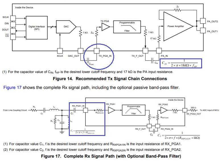
My customer is developing AFE032. As the internal DAC' s bit number cannot satisfy customer's requirement, so customer uses external DAC and feed the DAC output into the internal PGA.
To verify AFE032's own performance, customer disconnect the DAC output to internal PGA and leaves the TX_PGA_IN pin floating. Then customer did below program to AFE032:
Power up Initialization stage: Step 1~8
1. reg00->0x80; // Bit 7→1:Soft reset
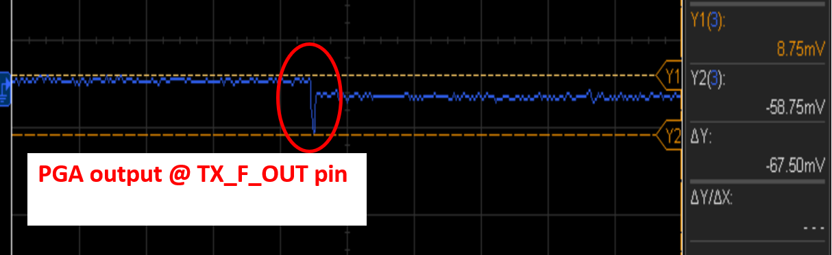
After this sentence is operated, we found the PGA output generate a spur

2. delayclk(66000拍)
3. reg08->0x1C; //Bit 4→1:PA_NRF enable,// Bit 3→1:TX_RX_NRF enable,// Bit 2→1:DAC_NRF enable
4.reg0F->0x11; // Bit 4→1:clk divider // Bit 0→1:clk divider
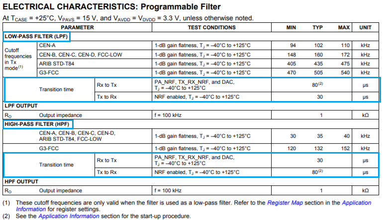
5.reg05->0x30; // Bits[6:4]→011:LPF=490kHz。
6.reg05->0xB0; //Set the Enable assist bit
7.Reg06->0x02 //Bits[2:0]→010:TX_PGA gain=3.25。
8.Reg03->0xE0 //Bit 7→1:LPF enabled //Bit 6→1:HPF enabled //Bit 5→1:Filter bias enabled
PA Enable Sequence: Step 1~10
1.Reg04->8'hB0; // Bits[7:6]→10:set PA Iq=95 mA。// Bits[5:4]→11:Set PA current limit=3.0A
2.Reg03->8'hB0; // Bit 7→1:LPF enable //Bit 6→0:HPF disable //Bit 5→1:Filter bias enable //Bit 4→1:PA enable
3.Reg06->8'h10; // Bit 4→1:TX_PGA enable, //Bit3→0: Rx disabled (default) // Bits[2:0]→000:TX_PGA gain=1.15
After this sentence is operated, we found the PGA output generate a spur
4.Delayus(53)
5.Reg03->8'hB4; // Bit 7→1:LPF enable //Bit 6→0:HPF disable //Bit 5→1:Filter bias enable //Bit 4→1:PA enable // Bit3→0: PA output stage disable
// Bit 2→1:DAC enable
6.Delayus(21.7)
7.Reg03->8'hBC; // Bit 3→1:enables the PA output stage
8.Reg04->8'hBC: // Bit 2→1:ENPAIQP // Bit 3→1:ENPAIQN
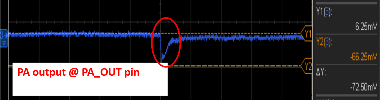
After this sentence is operated, we found the PA output generate a spur
9.Reg06->8'hD0; // Bit 7→1:ENPCOMP // Bit 6→1:ENNCOMP
10.Reg06->8'hD2 // Bits[2:0]→010:TX_PGA gain=3.25
So based on our test:
In Power up Initialization stage, After step 1 is operated, we found the PGA output generate a spur
in PA Enable Sequence, After step 3 is operated, we found the PGA output generate a spur. After step 8 is operated, we found the PA output generate a spur.
So can you help evaluate if this phenomenon is normal? Is it related to hardware or register sequence? Thanks.
Best regards,
Wayne