This thread has been locked.

If you have a related question, please click the "Ask a related question" button in the top right corner. The newly created question will be automatically linked to this question.

INAEVM-SO8: differential measurement by means of instrumenation amplifiers

Part Number: INAEVM-SO8

Hi,

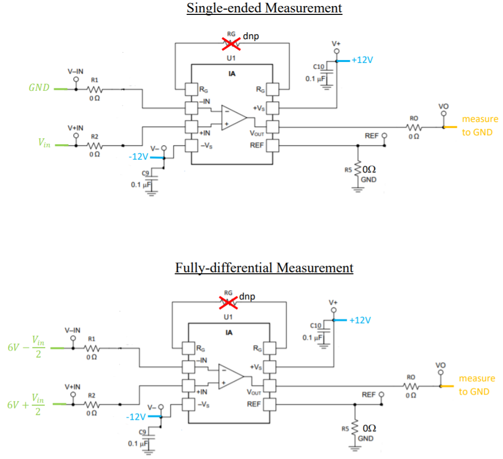
in order to implement an analog-to-digital conversion (input range of at least -6V to +6V) I wanted to check and survey some instrumentation amplifiers which are intended for driving the ADC. Therefor, I used the INAEVM-SO8 „Universal Instrumentation Amplifier Evaluation Module“. The INA129UA and the INA828IDR (gain=1, Vref to GND) instrumentation amplifiers were evaluated in dual-supply configuration and performed well in case of single ended inputs (error less than 1mV). In terms of measuring differential input signals the results, so the output voltages of the amplifiers (supply = +/-12V, common-mode offset = 6V), were not satisfactory. Permanently an error of at least 2mV (rather around 3mV) occurred. E.g.:

input: 0.05V -> output: 0.046V

input: 3.25V -> output: 3.2465V

input: 5.2V -> output: 5.197V

Since I only have 3-channel power supplies, I used two, one for the supply voltages and one for the input signals. As it can be seen in the attached photo, 1.004V instead of 1V was transfered to the amplifier input (upper power supply). Maybe this is a reason for the deviation of the amplifier output signal, but I am not sure what causes this effect (electric coupling on the evaluation board?).

Perhaps someone can help me ensuring better results in measuring differential signals by means of instrumentation amplifiers!

(If it is unsuitable to use the mentioned instrumentation amplifiers as ADC driver in an data acquisition system, please inform me.)

  • Hi Simon,

    how did you wire everything together? Can you show a plan?

    Kai

  • Hi Simon,

    Thanks for your post. I can help you.

    I've gathered the following information from your post:

    • gain = 1V/V 
    • ref = 0V
    • supply = +/-12V
    • vcm = 6V

    Can you send me a schematic of each configuration - single ended input and differential input? Please include the input voltage range for each. Can you also show how you wired everything?

  • Thank you for the help offered. 

    Here you can see how I performed the measurements:

    The black circuit represents the INAEVM-SO8 evaluation board and how I assembled it (Rg dnp to get gain of 1;  R5=0r to set REF to GND).  For U1 I used the two instrumetation amplifiers INA129 and INA828, as mentioned before. With an external power supply I applied +/-12V supply voltage (blue signals), with another one the input voltages (green signals) were applied.

    In case of the single ended measurement the IA output relatively accurate matches the input, in case of the fully differential one errors of a few millivolts occured.

    Simon

  • Hi Simon,

    the single-ended measurement has a smaller common mode input voltage to suppress compared to the fully-differential measurement. This explains why the output offset voltage error is slightly higher with the fully-differential measurement.

    But the main reason for the rather high error voltages (higher than specified in the datasheet) might be your improper measurement setup: I cannot see any shielding of the input voltage signals :-(

    The lack of shielding in combination with the lack input low pass filtering and in combination with the very high input impedances of INAs can result in input stage demodulation related error voltages caused by EMI hitting the unshielded input voltage lines. Demodulation effects manifest as unexplainable offset voltage degradation: The input or output offset voltages are higher than specified and can even show a "running away". Not only input voltage lines are susceptible to demodulation effects caused by EMI but also output lines...

    And last but not least, also the programmable DC power supply and the voltmeters can contribute to the offset voltage "error" due to their finite precision.

    Kai   

  • Hi Kai,

    thanks for your suggestions, I see the point that the input signalgs should be shielded and adjusted more concretely.

    Can you explain more precisely how I can implement this ideally for this circuit? I assume that a simple first order RC circuit on each input behaving as a low-pass filter might be an unsophisticated solution of filtering the signals. However, maybe you can recommend and present a convenient input stage circuitry (for shielding, filtering and so on).


    As an additional note:
    The evaluation board already offers the ability of input filtering (common-mode and differential-mode filtering), perhaps using it is sufficient.

    Simon

  • Hi Simon,

    R1 and R2 should be small enough to create no additional offset voltage caused by the voltage drop of input bias currents. Arround 2k2 might be appropriate here.

    Then, the corner frequency should be no higher then about 1/10 of unity gain bandwidth. A corner frequency of 100kHz might work here. So 1nF for C1 and C3 seems to be a good choice here.

    C2 can be made about ten times of C1 resulting in 10nF.

    I would take precision thin film resistors for the 2k2 resistors (+/-0.1...1%, +/-25...50ppm) and +/-1% NP0 caps for C1 through C3.

    Referring to the shielding of cables, use RG-58 or similar (need not to be expensive) and connect the shields at J1 through J3. Leave the shields unconnected at the DC power supply. You can connect signal ground comming from the DC power supply to one (but only one) of these shields, if you want.

    And: Increase RO to 100R :-)

    Kai