This thread has been locked.

If you have a related question, please click the "Ask a related question" button in the top right corner. The newly created question will be automatically linked to this question.

OPA348: Device Failure

Part Number: OPA348

Hey team,

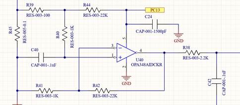
I have a customer who is having an issue with the OPA348AIDCKR - below is the circuit schematic.

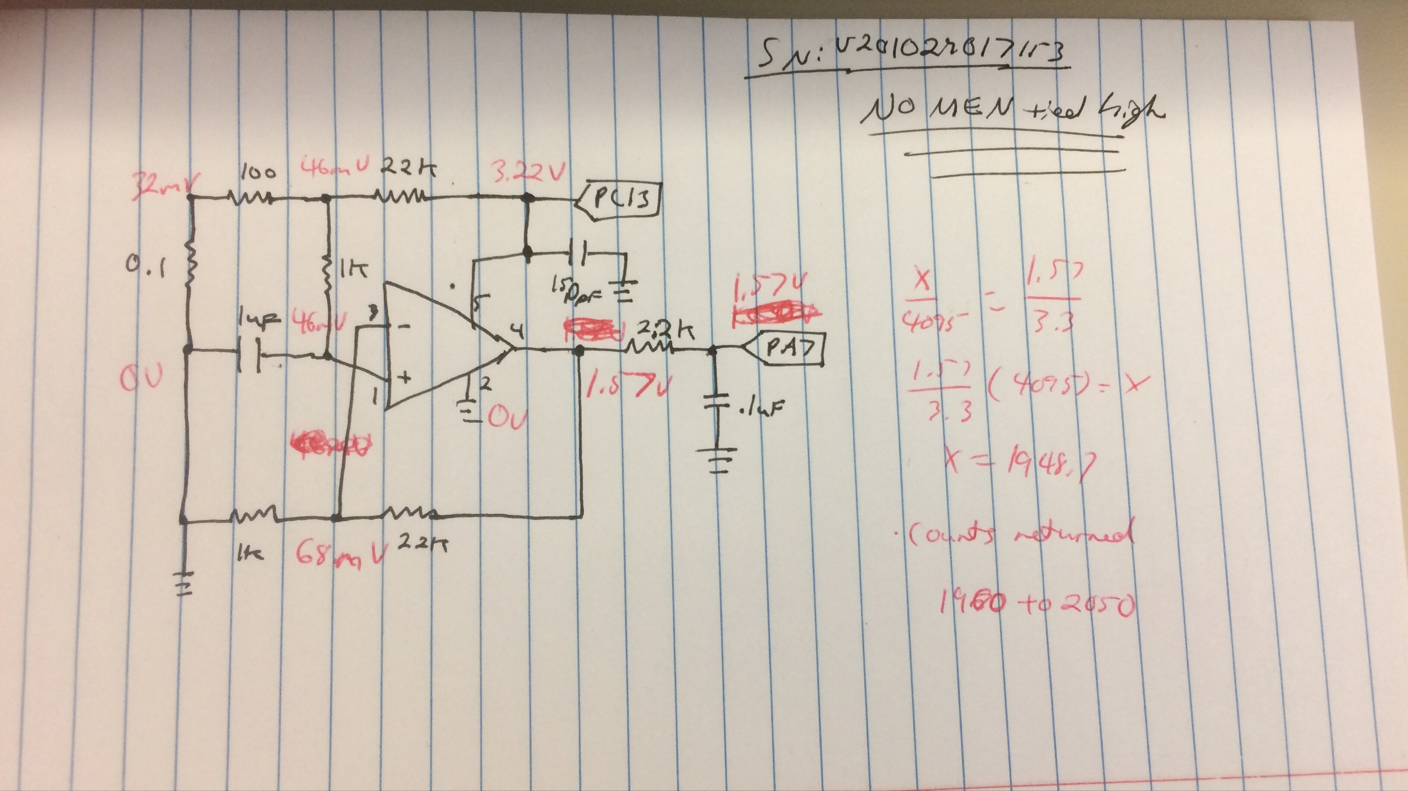
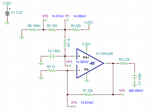
They verified that it is this part by swapping in a new op amp allowing the circuit to work however when swapping back in the old part it fails again.  On three of the boards they had a differential of 2-3mV on the inputs and the outputs were over 0.4V (expecting 344mV) though I think this is failing due to the enable not being able to be driven properly.  On the other two boards that failed the outputs were 2.8V and 3.28V on rails operating at 3.3V however the differential on the inputs was <1mv.

They were also curious about any part alternatives - the only parameters they can't afford to change are the input offset voltage and the rail to rail IO.

  • Former Member
    0 Former Member

    Hi Cameron,

    Thanks for reaching out.  I'm going to need a little more information to be able to help you here.

    First, can you post a more zoomed out view of the schematic?  I cannot see what the load is connected to.  But more importantly, I cannot see the input.  While I can guess with reasonable certainty, it's best not to assume.

    Second, what is the input voltage?  Is this intended to be a purely DC circuit or is it an AC signal and what are the voltage levels?

    Third, when they swap in a new op amp is it a different part altogether or just a different unit but still the OPA348?

    Additionally, when you mention "failing due to the enable not being able to be driven properly," which enable pin are you talking about here?  The OPA348 has supply pins but no enable pin.

    As far as I understand, you are expecting an output voltage of about 344mV (DC).  But three boards are giving you a DC voltage greater than 0.4V and two other boards are approaching the V+ rail.  Please correct me if I am mistaken.

    I will be happy to suggest a different part, if that is what is desired.  But, we probably need to find the issue first or we'll be shooting in the dark.

    Regards,
    Daniel

  • Former Member
    0 Former Member

    Cameron,

    One more thing: is a voltage provided to the supply through PC13?  Or do both the input voltage and supply voltage come from the far upper left of the schematic?

    Regards,
    Daniel

  • Hey Daniel,

    Thanks for the response - they're primarily looking for a newer part that would be a drop in replacement I think. 

    1. Can we get a more zoomed out view of the schematic? We’re unsure what the input looks like / is – also is this a purely DC circuit or is there an AC signal involved?
      1. Some of those initial values are off based on how I was testing it.  I reran it in a more realistic way and here is a breakdown of the voltages.  As you can see we are actually getting a 22mV differential between the inputs.
    2. I assume when you mentioned you switched the chip and it is working that you switched it with another OPA348, but just wanted to confirm.
      1. Yes I’ve swapped the chip out with another one and the circuit operates as intended, and then swapped back in the original part and it fails.
    3. What is the enable you are referring to below that you thought might be the issue?
      1. No longer an issue
    4. Is a voltage provided to the supply through PC13 or do both the input voltage and supply voltage come from the far upper left of the schematic?
      1. See attached
    5. Just confirming the problem statement: You are expecting an output voltage of about 344mV (DC).  But three boards are giving you a DC voltage greater than 0.4V and two other boards are approaching the V+ rail. 
      1. With the new data the problem statement should be more along the lines that we are seeing too large of a differential between the inputs (this part is spec’d at 6mV from what I’m seeing in the datasheet)
        I’ve also brought it up on a scope and I’m not seeing any oscillations on the input

  • Former Member
    0 Former Member in reply to Cameron Perl

    Hi Cameron,

    Thanks for the extra information here.  The strange thing is that it looks like the DC biasing points are off.  For example, take a look at the resistor network that is connected to the non-inverting input.  The voltage at the 22k resistor should be about 14.58mV just by the resistor divider alone.  Also, the voltage above the 0.1Ohm resistor should be nearly 0V.  I'm not sure how there could be 32mV there.  Even if the offset voltage of the amplifier is off for some reason, I wouldn't expect to see these values.

    Here's an image of the simulated DC biasing point along with the simulation file.

    Cameron_Perl_OPA348.TSC

    Regards,
    Daniel