This thread has been locked.

If you have a related question, please click the "Ask a related question" button in the top right corner. The newly created question will be automatically linked to this question.

OPA837: Circuit simulation.

Part Number: OPA837
Other Parts Discussed in Thread: OPA832

Hi community,

I hope everyone is safe at the current time.

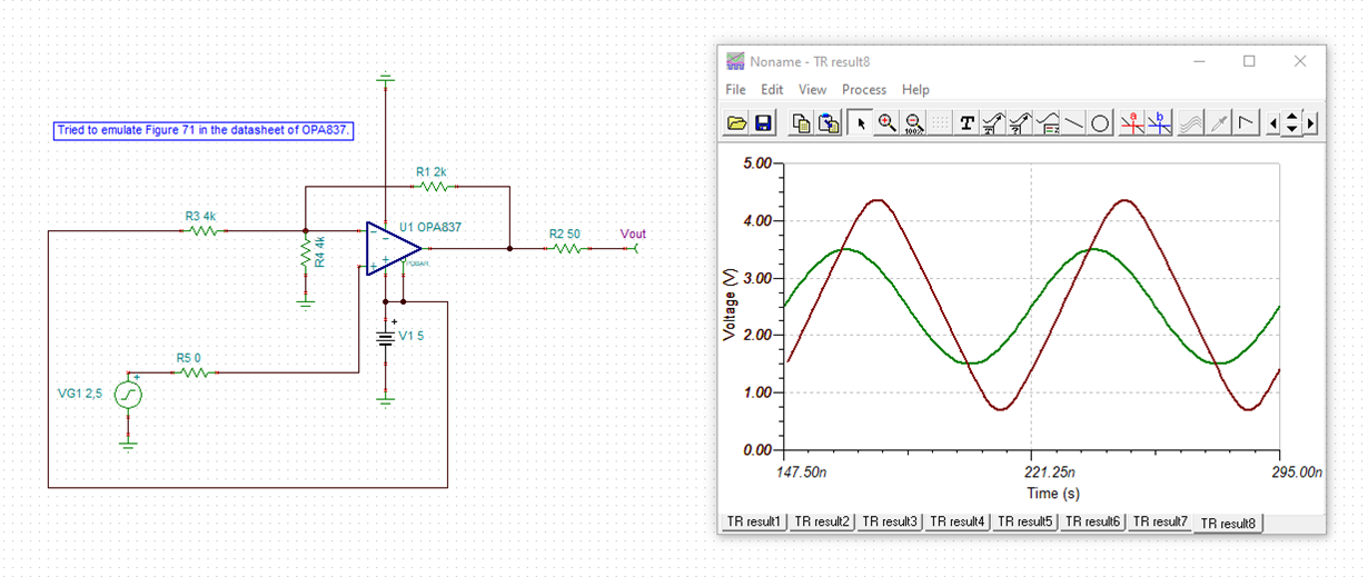
Actually, I was trying to design a buffer and LPF circuit with a single-supply design using OPA837 op-amp and I tried to follow Figure 71 in the datasheet for the buffer circuit, however, I failed to get the desired output out of it. I also tried with dual-supply where it works fine. Can anyone help me to sort it out? File attached for buffer circuit (In reference to Figure 71 of the datasheet). OPA837_SingleSupply.TSC

Thanks in advance.

Best regards,

  • If you look close Gyan, that input signal is shown at 2.5V DC incoming, here I made that change, works fine, You always have to watch out for I/O headroom limits, 

  • Hi Gyan,

    you input signal wasn't centered arround midsupply but arround 0V. By this you violate the common mode input voltage range of OPA837. Also, R5 = 1k made trouble in the simulation. So I reduced R5 to zero:

    gyan_opa837.TSC

    Take care, the spiky sine indicates that the OPA837 is not fast enough for your application.

    Kai

  • What Kai means by spiky is that output waveform looking more linear on the transition that sine wave, yes, your input transient condition is pushing towards 200V/usec slew rate demand while that device only has 105V/usec available, reduce the swing or frequency to get back into range. The model is doing a great job of showing this. 

  • Dear Michael and Kai,

    Thank you for your kind response.

    Since my input will be centered at 0V, is there a way to modify this circuit with a single input supply?

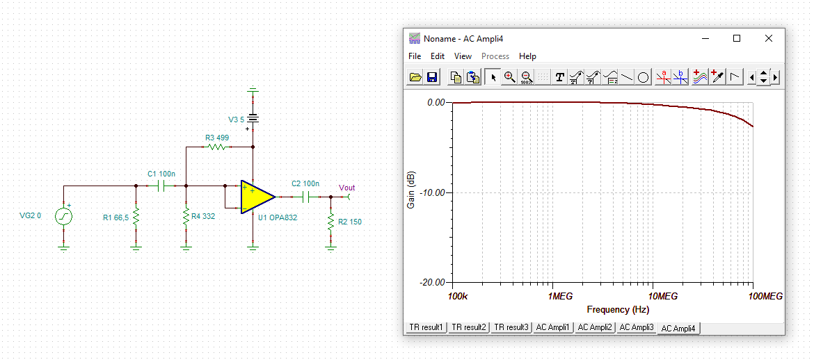
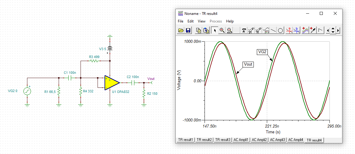
    Something like with OPA832 in the attached file. However, I can not increase the gain though.

    Thank you.

    Best regards,

    UnityGain_OPA832.TSC

  • Hi Gyan,

    looks better now:

    What is driving the input of OPA832? Is there a cable?

    Kai

  • Hello Gyan,

    You will need to center your input & output signals around mid-supply in order to not exceed the in/out limitations of the device. The OPA832 circuit is AC coupling the input and referring it to mid-supply.

    You also mention a LPF, is that a part of this design or will you be adding that to a following stage?

    Best,

    Hasan Babiker 

  • Dear Kai,

    Thank you for your kind response. I gonna apply it to the RF receiver circuit.

    Here, I would like to increase the gain of the buffer but not able to do so.

    Any idea!

    Best regards,

  • Dear Hasan,

    Thank you for your response.

    Well, in my RF receiver circuit, I gonna use a buffer with a certain gain (say G=2) and then use an LPF to filter having a center frequency of about 40 Hz to filter out the power signal noise (say 50-60 Hz) but with a single supply mode.

    I also prefer to use only one OPAMP model, if possible.

    Any suggestions will be welcomed.

    Best regards,

  • Hello Gyan,

    Can you clarify as to why you are simulating with a 13.56MHz signal if you plan to add a LPF with a cutoff frequency of 40Hz? Did you mean high-pass?

    Also, you are trying to amplify the signal at a gain of 2 right? When you say buffer, this means unity gain (G = 1).

    Are you using the OPA837 or OPA832? The schematic needed for each of these devices is different as the OPA837 is a typical amplifier & the OPA832 has an internal gain and feedback resistor. 

    Best,

    Hasan Babiker

  • Hi Hasan,

    Thank you for your response.

    Let me clear up with the following:

    1. Well, the reason behind using 13.56 MHz input is to use for NFC carrier. Since this circuit is for low-frequency sensors (say pulse rate measurement) I am using a buffer in front of the envelope detector and LPF after the envelope detector circuit to filter out the power noise. 

    2. Regarding the use of OPAMPS, I am open to any type (you may recommend some better options as well) but I would like to use the same OpAMP for both of my requirements (buffer and LPF) and operate with a single power supply (+5 V). The amplification purpose is just to increase the SNR.

    Best regards,

  • Hi Gyan,

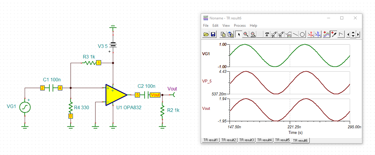
    you could do it this way:

    gyan_opa832.TSC

    Kai

  • Dear Kai,

    Thank you very much for your suggestion for designing a buffer amplifier with Gain=2.

    Any suggestion about the LPF (cut off 40 Hz) using the same OPA832 opamp (with gain = 10) and with a single supply?

    Best regards,

  • Hi Gyan,

    I leave it to you, as an excercise :-)

    Kai

  • Hello Gyan,

    You won't be able to achieve a gain of 10 with the OPA832 as this is a fixed-gain device (supports gains of +1, -1 & +2). You can configure a normal amplifier to a gain of 10 and use ac blocking caps at the input/output as Kai as done here. Then follow this up with a passive LPF. Or you can use a bandpass MFB filter. The OPA832/OPA837 are much higher in bandwidth than you require so you may want to look at lower frequency devices that better meet your preferences (noise, power consumption, cost, etc.).

    Best,

    Hasan Babiker