This thread has been locked.

If you have a related question, please click the "Ask a related question" button in the top right corner. The newly created question will be automatically linked to this question.

THP210: Input common mode voltage

Part Number: THP210
Other Parts Discussed in Thread: OPA189, , ADS1261

Hi TI,

I am building a circuit to sense a current with requirements as below:

- Sensing current: 100uA-1A 

- Input common mode voltage: 1V-5V.

-Output voltage swing: +/-2.5V (diff)

-Output common mode voltage: 2.5V

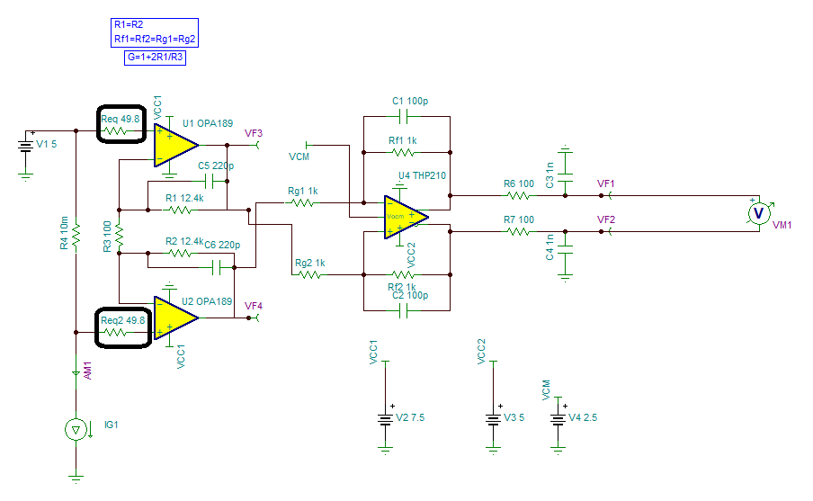
I start with TINA simulation (see picture)

I can see VF3 is bigger than VICM range of U4 (VVS– + 1 to VVS+ – 1) and even VCC2 when IS1>=1A. Is it OK? I can see it seem to be no problem in the simulation.

And how do you think about this circuit? Are there anything should to be noticed?

Thank you,

OPA189-THP210 diffamp.TSC

  • Hi Vo,

    the common mode input voltage range of THP210 wouldn't be violated. See "VF5" and "VF6":

    Kai

  • HI Vo,

    The VICM refers to the input common-mode voltage right at the input terminals of the THP210 Fully-Differential Amplifier.  The specification on pg 5 of the datasheet defines the VICM valid range as (V_VS-) + 1V <VICM < (V_VS+) - 1V; where this is the input common-mode voltage right at the input terminals of the THP210 need to be at least 1-V from both supply rails.

    As Kai has shown on simulation, the THP210 VICM voltage on the circuit above is ~3.747 when the current across the shunt is 1A, and 3.7495V when the current is 100uA, there is no violation of the THP210 VICM range on the circuit above.

    Thank you and Regards,

    Luis 

  • Thank you for your quick reply. I have build a HW and done some measurements. The result is hopeful.

  • GAIN= 250.50
    Rload Notes ADC Data VM1 (V) VM1-Voffset (V) I (R4) (A) AM1 (A) error
    V1=2.5V
    infinity Voffset= -16846 -0.005020
    10K -14735 -0.004391 0.000629 0.000251 0.000250195 -0.37%
    2k2 -7222 -0.002152 0.002868 0.001145 0.001144 -0.08%
    250 68208 0.020326 0.025346 0.010118 0.01 -1.18%
    V1=4V
    infinity Voffset= -18356 -0.005470
    10K -15067 -0.004490 0.000980 0.000391 0.000400219 2.24%
    2k2 -2725 -0.000812 0.004658 0.001859 0.0018255 -1.86%
    250 117945 0.035148 0.040618 0.016215 0.0159971 -1.36%
    V1=1V
    infinity Voffset= -15711 -0.004682
    10K -14949 -0.004455 0.000227 0.000091 0.000100159 9.49%
    2k2 -11806 -0.003518 0.001164 0.000465 0.00045463 -2.18%
    250 18275 0.005446 0.010128 0.004043 0.0040056 -0.93%

    Hi TI,

    I'd like to use this thread again to ask you about the noise voltage at the output of this circuit and to show the result of measurement.

    I replace IS1 with Rloads (Infinity, 10K, 2.2k and 250ohm).

    I use ADS1261 EVM in place of VM1 and a high accuracy ammeter in place of AM1. (This AFE is intended to use with a simultaneous sampling ADC not ADS1261)

    When Rload=infinity, there is a noise voltage measured at the output as shown in the table above (bold numbers). It is about -5mV. How can I reduce this noise?

    Thank you

  • Hi Vo,

    you could decrease the bandwidth of your circuit - and by this the noise - by giving all the feedback caps a value departing from zero :-)

    What bandwidth do you need?

    Kai

  • HI Vo,

    Depending on the bandwidth required on the application, you would need to set capacitors C5, C6 at the feedback of the OPA189 stage and capacitors C1/C2 at the feedback of the second THP210 stage, as well as the RC filters at the output.  The overall noise of the circuit will be dominated by the OPA189 differential gain stage. 

    If you need assistance, please let us know the bandwidth required in the application.

    Thank you and Regards,

    Luis

  • Hi Luis,

    I use this AFE +ADC to measure current consumption of Wifi/Bluetooth device, BW=30kHz should be sufficient. A input filter to filter out noise before amplifying is what I am thinking. I have examined the waveform which displaying on "Delta-sigma ADC Evaluation SW", -5mV is not only noise, It includes noise and DC offset. With the gain=250.5, the input offset + noise is about 20uV. It would be big number for a low noise, low input offset Op-amp like OPA189.

    Thanks,

  • Hi Vo,

    In order to reduce the noise, a couple of things to try:

    1)  Reduce the R1, R2, and R3 on input stage to reduce resistor thermal noise and effect of current noise of the amplifier interacting with the resistors.

    For example:  R1, R2 = 12.4kΩ and R3=100Ω

    2)  Depending on the bandwidth required on the application, set capacitors C5, C6 at the feedback of the OPA189 stage and capacitors C1/C2 at the feedback of the second THP210 stage, as well as the RC filters at the output.  The overall noise of the circuit will be dominated by the OPA189 differential gain stage. 

    3)  The OPA189 is a chopper amplifier.  In order to match the impedance on inputs to reduce chopper errors / IB spikes effects, we add an equivalent matching resistance Req1 and Req2.  The chopper noise comes from the input current spikes generated by closing/opening of the front-end switches at the chopper op amp input terminals.  The source resistance and feedback resistors convert the IB spikes into voltage spikes.  Therefore, in order to minimize the magnitude of the error, one needs to balance the input impedance at each input terminal by adding equivalent resistors. You could read more about noise in chopper amplifiers on this E2E post. In the example above, the equivalent resistor would be

    REQ = 12.4k || (100 / 2)=49.8Ω

    The example below has f(-3dB) = 36kHz and Total Noise of OPA189 + THP210 stage of ~295uVRMS:

    Alternatively, you could build a similar circuit with a standard linear amplifier and re-adjust the capacitors accordingly (you will not have to add the matching resistors Req1 and Req2 for the standard linear or non-chopper amplifier)

    The bandwidth is about f(-3dB) = 36kHz and noise is about 330uV-RMS

    Thank you and Regards,

    Luis Chioye