This thread has been locked.

If you have a related question, please click the "Ask a related question" button in the top right corner. The newly created question will be automatically linked to this question.

TLC2272: negative voltage sample

Genius 3870 points
Part Number: TLC2272
Other Parts Discussed in Thread: TINA-TI

Hi there

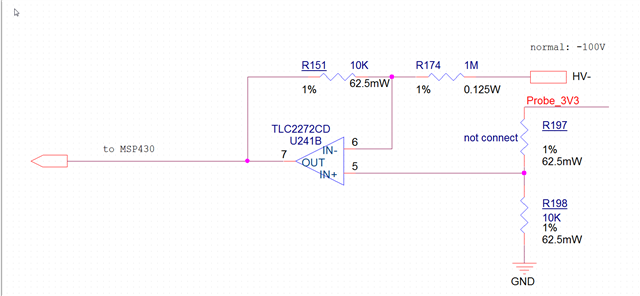
we are plan to use TLC2272CD to sample -100V power. As bellow SCH, can we just connect the + input to GND (R197 not connect , so V_moni = -0.01 * HV- ) ? 

or do we need to solder R197 as 10K in order to provider some DC bias ?   Thanks!

  • Hello XY,

    If I understand your question correctly you are asking if the TKC2272CD non-inverting input should be connected to ground through the R196 10 k resistor, or can it be connected directly to ground without R196?

    Either will work, but connecting the non-inverting input directly to ground eliminates the thermal noise generated by the 10 k resistor. Doing so reduces the noise a little in the op amp circuit which should be desirable. 

    Regards, Thomas

    Precision Amplifiers Applications Engineering

  • Hi Thomas, thanks for answer. 

    I think I forget to tell you the power supply condition of TLC2272. it is supplied by SINGLE +5V. So my question is , which configuration is better? 

    (1) R197 DNI(do not install), R198=10K or 0,  this means non-inverting input is grounded.  and as you said, grounding pin5 directly leads to less noise. Although TLC2272 is a rail-to-rail product, but I still need to confirm it can accept non-inverting input as low as GND.   

    (2) R197 = R198=10K , so this means non-inverting input is biased to 1.65V. 

    Thanks.

  • Hello XY,

    The TLC2272 should work in either case as long as its input and output limitations are observed. I put together a TINA-TI circuit and simulated the output for an input range of -100 V to 0 V.The first circuit has the TLC2272 non-inverting input grounded (Vcm = 0 V), and the second TLC2272 circuit having the non-inverting input biased at 1.65 V by the 10 k resistive divider (Vcm = +1.65 V). You can see the results below for the two conditions.

    The lower curve shows that the output is 1.00 V, when the input is -100 V, and moves downward to about 10 mV when the input is 0 V. It doesn't quite make it to 0 V because the TLC2272 output can't swing all the way to 0 V. The upper curve is the output with the +1.65 V common-mode voltage applied to the non-inverting input. The output is about 2.67 V, when the input is -100 V, and moves downward to about 1.67 V when the input is 0 V. The main thing to watch when applying a common-mode voltage (Vcm) to the non-inverting input is that the maximum positive limit not be exceeded. The datasheet electrical characteristics table indicates that is 1 V below V+.

    So it looks like either connection will work you just need to decide which range is correct for your application.

    Regards, Thomas

    Precision Amplifiers Applications Engineering

    TLC2272_Hi NegV In_01.TSC

  • Hi Thomas, thanks for help. An extended question to cousult.

    When input is 0V, the ouput of upper circuit is 9.237mV as you mentioned TLC2272 output can't swing all the way to 0 V. But the datasheet claims it output Swing Includes Both Supply Rails. So this rail- to- rail is non-ideal. So what parameter should I look into in order to determined the upper and lower output voltage range?

    Besides of the non-ideal rail-to-rail performance, If I also take the Vio(input offset) (max. 2500uV) into consideration, the output offset when input=0V should be 2500uV*(1+0.01) = 2525uV.

    Thanks again.

  • Hello XY,

    The output voltage swing of Rail-to-Rail specified op amps is never exactly to the supply rails because the output transistors, in this case MOSFETS for the TLC2272, have a finite amount of ON resistance (RON). That is why the TLC2272 model is bottoming out at about 10 mV above ground (0 V) in the circuit. The more current demanded by the load the less close to a supply rail the output will swing due to the voltage drop across the output MOSFETS RON resistance.

    The VOH and VOL parameters in the electrical characteristics provide the output voltage (Vo) swing characteristics. You can see that potion of the TLC2272 table below.

    Yes, the input voltage offset Vio could be a factor affecting the output Vo as well. If the input offset to positive as you have indicated that would add to the VOL level. If however, the input offset were negative by the same amount the output can't swing below its lowest VOL level.

    Do note that the maximum and minimum VOH and VOL levels are what we refer to as "slam" levels. The op amp output is slammed as close to the supply rails as it can go. This is essentially saturation and the output is no longer operating its in linear region. The true linear output operating range is that listed in the AVD large-signal differential voltage amplification.portion of the table.

    Regards, Thomas

    Precision Amplifiers Applications Engineering

  • Hi Thomas, thanks for patient explaining. That's helpful.

    Just to confirm, I think the "AVD large-signal differential voltage amplification" you mentioned above is the same parameter as Open Loop Gain. And I found TLC2272 Avd is typ.35V/mV( 91dB) at RL=10Kohm , it is smaller than most general OP amps in out library ,which is generally >100dB. However, when at RL=1mohm TLC2272 Avd is typ.175V/mV(105dB), this is bigger, but the load resistor seems too small. I doubt whether TLC2272 could bear 1mohm.

    Thanks.

  • Hi XY,

    Yes, the AVD parameter listed in the TLC2272 Electrical Characteristics table is the open loop gain parameter. The TLC2272 uses a N-ch/P-ch, drain-to-drain output stage that develops a voltage gain that is a function of the load resistance applied to the output. The voltage gain it develops contributes to the overall open loop gain (AVD) of the Op amp.

    Figure 24, Large-Signal Differential Voltage Amplification vs Load Resistance, shows how dramatically AVD is affected by the load resistance RL. A high resistance RL load results in much higher AVD than a lower resistance load as the graph indicates. Do note that the Figure 24 horizontal scale is kilohms so the lowest resistance point on the curves is 300 Ohms. That is not really a practical load resistance for the TLC2272 compared to the 10 kilohm load specified in the Electrical Characteristics table for AVD.

    Regards, Thomas

    Precision Amplifiers Applications Engineering