


Hi,
in AMC1200 datasheet Figure 32. Typical Application Diagram, there are C3 from VINN to GND and C4 from VINP to GND, and it's said to be optional.
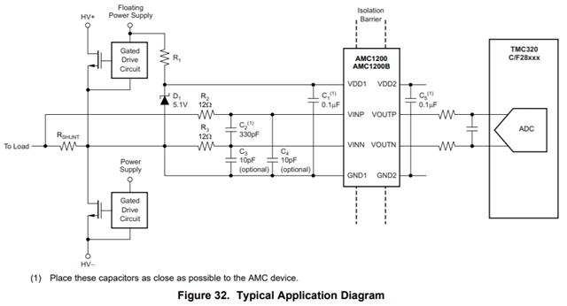
Optionally, C3 and C4 can be used to reduce charge dumping from the inputs. In this case, take care when choosing the quality of these capacitors; mismatch in values of these capacitors leads to a common mode error at the modulator input. If implemented, TI recommends using NP0 capacitors for C2 , C3 and C4.
I don't understand what does charge dump mean here. Does it mean that in Sample and Hold stage, the internal capacitor is charged through C2 and C3? But we've already have CINP and CINN=3pF here, which should have the same effect as C2, C3.
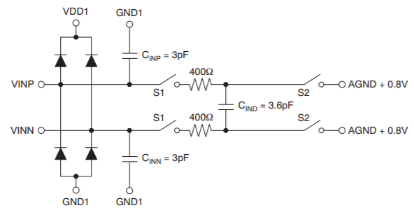
And the customer also asks how we do the sample, is it that we get (VINP-VINN) analog signal and then do the digitization, or we digitize VINP and VINN seperately and then do the subtraction with the digitized value?
I guess it's the first case, during the sample and hold stage is: CIND is charged to VINP-VINN, and then this analog signal is digitized, right?


