


Other Parts Discussed in Thread: LM393, LM293, LM139, LM339
Hi team
Question 1:
Refer datasheet SLCS005Z –OCTOBER 1979–REVISED OCTOBER 2017.
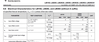
Table 6.6. Electrical Characteristics for LM193, LM293, and LM393 (without A suffix)
at specified free-air temperature, VCC = 5 V (unless otherwise noted).
The first 3 rows of this table (Parameters Vio, Iio, Iib) all mention the test condition of Vo=1.4V. Since the supply voltage will be 5V at minimum, I am curious about this value of 1.4V, since is an intermediate voltage level (not 0V, and not Vcc), which seems to suggest that the output NPN transistor is being kept in its active (linear) state as part of the test fixture (or that it is fully ON and is conducting far more than 4mA - very unlikely). Is that the case? If so, what is the current flowing into the output pin in the test? Why is the value of 1.4V used here? Does changing either Io or the 1.4V value influence these parameters? For example, suppose Vcc=12V, and I wanted to know these parameters when Vo=6V(Vcc/2), do these parameters change significantly? Does changing the output current (collector current of the output transistor) also affect these parameters?
Question 2:
Let's assume that Vcc=12V, the output has a pull-up resistor of 10k to Vcc & there no connection of output to either input, and the positive input (pin 3) is held at 1.0V. The negative input (pin 2) is now ramped from 0V up to 5V. How does the current of pin 2 (neg input) change during that ramp?
Please kindly give your comment.
Best regards
Lidong

 add screen shot for your reference.


