This thread has been locked.

If you have a related question, please click the "Ask a related question" button in the top right corner. The newly created question will be automatically linked to this question.

TPA6120A2 headphone amplifier power supply capacitance for the output THD specified

Other Parts Discussed in Thread: TPA6120A2


 Dear TI audio IC designers,


We need in TPA6120 headphone amplifier additional information:


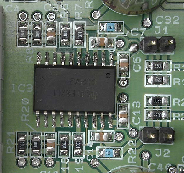
There is power supply capacitance of low ESR 100uF electrolytic on each rail at the TPA6120A2 headphone amplifier datasheet application circuit.

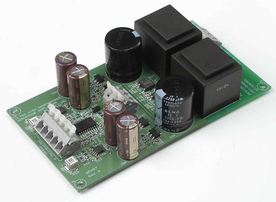
There are such power supply capacitors on the TPA6120A2 Evaluation Module schematic (slou169 document).


Unfortunately, the TPA6120A2 Evaluation Module user’s guide has no information regarding its real THD specification.


Is it enough the TPA6120A2 power supply capacitance of those low ESR 100uF on each rail to keep the headphone amplifier THD value (in full sound bandwidth range) at the datasheet listed level and load resistance of 70..300 Ohms?


The TI audio forum (in the Audio FAQs ) has some considerations on this subject:


***********************************************

How can I improve low frequency THD+N in my design?

If you changed PVDD capacitance, you can see increase THD+N at low frequency input case and also this value depends on channel separation factors. If someone would like cost reduction by decreasing PVDD cap value and size, should check low frequency vs THD+N spec before changing capacitance.

http://community.ti.com/forums/t/2645.aspx

***********************************************


Sincerely,
 
Alexander M.
  • Alexander, the decoupling shown in the TPA6120A2 users guide, including the 100uF caps, is specified because of the low THD the part produces.  It should be enough to maintain performance of the device .  Since the device is a headphone amplifier, power supply current is fairly low, and the decoupling shown is adequate for that application.

    Best regards,

    Steve Crump.

  •  

    Hi, I have one of the eval modules, and was wondering what is the max current that I should allow, when powering up the module?

    I have a +15V/-15V supply ( rated for 0.5A ) and noticed that just power up the board ... w/o connections, the part get exceedingly hot!!!!  & even noticed that the resistor ( R8 on RIN+) started to smoke!!  

    What am I doing wrong?


    // Sal 

  • Sal, I don't think the issue is with the power supply, unless it is actually delivering more than +/-15V.  You might verify that, but it's probably not the problem.

    Maybe it's the power supply connections to the EVM?  With proper connections the EVM should power up nicely without heat or smoke, drawing less than 30mA.  But check your connections to make sure nothing is swapped, including swapping ground for +15V or -15V.  Maybe verify with a DMM.

    If that all checks out, then obviously the problem is in the EVM, and you need to swap it for a new one.

    I hope this is helpful to you.

    Best regards,

    Steve Crump.

  • Thanks for the feedback.  I have built my own board based on the EVM.  I am supplying +/-15V DC.  In my first prototype, I was unable to solder well the GND pad on the bottom to my board.   I got it built.  And I am testing it, but I noticed that if I supply a sinusoid of 390mVRMS, I and Monitor the output ... The part gets hot and the output voltage gradually drops.  Is this strictly due to the incidental connection to GND on the bottom, or what else do you think I've done wrong?  I am measuring 0.30mADC on the -15VDC supply, and 0.70mADC on the +15VDC, using a Fluke 179 true rms DMM (connected to the 400mA port).

    // Sal Aguinaga

  • Sal, I will guess the problem is either the missing PowerPAD connection on the bottom of the device, which leaves it without heatsinking, or oscillation, because of some circuit problem.  Is there any way you can send me your schematic and PCB layout in PDF, as well as describe your load?

    You had a problem earlier with an EVM, with the device overheating and a resistor burning.  Were you able to sort that problem out?

    Best regards,

    Steve Crump.

  • Thanks for the reply, first, I did sort out the issue with my earlier post... It was not the EVM, it was my rev A board and my bad solder-job.

    Yes, I can give you a copy of my schematic and send the gerber files.  Let me know where to send that to.


  • Sal responded outside the audio community, so he could send files.

    I have a Single channel signal ( in differential mode) coming into each of the XLR/TRS combo connectors, and I am using each amp to do 2x gain on the signal and sending it to a XLR connector, then 'T' off to a TRS output connector, but I want to limit the abs max voltage on the TRS (actually a TS) to under 2VRMS if the input signal is +/-12V peak, so I'm using 2W 25 ohm resistors in series so that a 10 ohm speaker/transducer is the load on the TRS output connector.

    I've assembled the prototype myself, but since I don't have the right tools, I did not make a good (or any) connection between the bottom pad of the IC and the pad on the board.

    On the input side, I have options to populate a board with PCB-mounted TRS/xlr connectors, or put the connectors on a panel and then wire them them to the 3-pin thru-hole connectors (like J41).

    Please, let me know if you have some questions or if there are any issues with the files.

    // Sal Aguinaga
    // Northwestern University

  • Sal, your schematic looks fine except for one item: the power supply decoupling you show includes only 0.1uF capacitors on each amp for each supply.  Our EVM uses a 10uF ceramic cap and a 100uF electrolytic on each supply, in addition to the 4 0.1uF.

    Can you try adding at least the 10uF caps?  If that doesn't fix it, I think the issue must be that the PowerPAD is not soldered.  It is a critical thermal contact, but it has electrical requirements as well.

    Best regards,

    Steve.

  • Sal, in case the issue proves to be soldering the PowerPAD, I tracked down an inexpensive hot air tool that I bought some time ago for desoldering and soldering ICs.  This was a model AT85028, a hot air station with 8 nozzles, from Madell Technology, http://www.madelltech.com.  It cost $250, and it is easy to use.  I have successfully desoldered and soldered a number of ICs with it.

    I don't know if this can fit your budget, but I wanted to suggest it.

    Best regards,

    Steve.

  • Hello Steve,

    On page 3, I have the supplies and their decoupling ... each one with a 10uF ceramic and an electrolytic, so it looks like it is strictly a function of the thermal pad?  Let me know if you can thing of something else I should try.

    I'll wire up another board to see if I can improve it.


    Thank you. // Sal

  • Sal, thanks for the PCB layouts.  I checked them and compared them to the EVM, and I see no big difference.  Your layout follows the EVM layout and the guidelines for it closely, including observing the warning to avoid putting ground plane under the input pins of TPA6120A2 and connected leads.  (The device has very wide bandwidth, 100MHz or so, and even small capacitances at those points can reduce phase margin.)

    So I think the problem is not your layout, or your decoupling (which certainly includes all the expected caps).  I am investigating whether a floating PowerPAD can cause electrical problems, but we know that it will cause thermal problems with reasonable loading.  (BTW, I'm not sure I know the load you are using - please let me know.)

    Is there any way you can be sure of soldering the PowerPAD?  Do you have access to a hot air gun for this?

    Best regards,

    Steve.

  • Hi!

    I got ahold of a heat gun and first soldered each of my ICs to the board (4ch) and then I soldered each of the parts for one IC (so the only load on the power supplies is 1 IC).  I made a comparison between the EVM and my board (so I used the same power supply, the same headphones load, and the same signal generator).  Once again ... My board sounds great, when I load it with a 1K tone at 302mVrms (input), but after a while .... the chip gets super hot (uncomfortable to the finger after a few seconds)!  Both the surface of the IC and bottom side of the board under the belly of the IC, are very hot.  The current I measured is 2.1 and 2.0 mA DC when measured across the ferrite bead ( is this the correct current draw measurement?).  One of the differences between the EVM and my board, is that my board has a thermal pad connected to the Bottom side GND by only 4 vias.  The thermal pad is an actual pad, member of the footprint, where as Ti's looks like instead of a 'pad' it has a set of vias (21)  added to connect Gnd top and bottom, and the footprint only has a mask-clearance?  Do you have pdf version of your footprint?

    Would it be okay to use a 10ohm, passive, load on the output connector?  Any other ideas will be greatly appreciated.

    // Sal

  • Sal, the PowerPAD must be soldered, as you know, and 4 vias may be too few.  There are 2 pieces of information you need to get the PowerPAD connection right.

    - The layout of the via array.  See slma002A, page 9, left side about half way down the page.  There is a via array layout for SSOP, DWP20, TPA6120A2 package.  It includes a 3x6 array of 18 vias for the SSOP DWP20 package for TPA6120A2.

    - The size of the PowerPAD solder area.  That same page in slma002A says "The maximum exposed pad size listed in the datasheet should be used to design the solder mask defined pad. Solder mask defined pads are recommended to prevent shorting between exposed pad and package leads".  The maximum exposed pad size in TPA6120A2 data sheet, slos431, 2.54mm x 3.3mm, is shown on the 25th page of the data sheet under THERMAL PAD MECHANICAL DATA.

    - The size and spacing of the thermal vias.  These should be 0.33mm, too small to wick solder, but large enough for good thermal conduction, placed on a 1mm grid.

    I don't have the actual layout.  I can track it down if necessary, but it will show a solder pad (mask opening to tinned copper) like the one described above.

    Back to the remaining problem, overheating of the part.  I need you to clarify some items for me.

    - I expect you've operated the EVM as you operate your circuit.  Is it correct that the EVM does not lose output voltage, and the device doesn't heat up, including the bottom side of the PCB opposite the PowerPAD?

    - You say you measure "2.1 and 2.0 mA DC when measured across the ferrite bead".  I take it you mean the ferrite beads you have placed between +/-12V power supplies and 12VP/Nx.  How are you measuring this?  The correct method would be to lift a bead, resolder one end, and place the Fluke meter current port between the bead and the power supply, with the meter set for several hundred mADC to an amp DC or so.  I assume this is what you're doing.

    - The numbers "2.1 and 2.0 mA DC" don't quite make sense, because quiescent current of TPA6120A2 is 11.5mA typical per channel, 23mA typical per package.  Can you check this?

    - I don't know your load or output voltage.  Can you tell me these?  I'd like to know inductance as well as resistance of the load resistor you're using, if you can determine that.

    (TPA6120A2 absolute minimum load Z is 8ohms, but minimum recommended load Z is 16ohms.  Working with less than the minimum recommended load will cause erratic operation, so I think a 10ohm load is not a good idea.  But did you not have series 25ohm resistors in your circuit for feeding a speaker load?)

    - We know your PCB is not laid out according to slma002A.  However, rather than trying to modify a PCB at this point, maybe you can add a small heatsink on top of one of the chips, and see if that keeps TPA6120A2 happy.  Try the easiest heatsink to find as a start.

    - A final step at this point would be to check your output with a scope while you are driving it at your present output.  I'd like to be sure the device is not oscillating at some point in the cycle.

    If we can get good current measurements, and you can try the heatsink experiment, check the output voltage with a scope, and tell me your output voltage and load, maybe we can understand this.

    Best regards,

    Steve.

  • Hello,

    Thanks for the info on the thermal pad layout.  I want to answer the question about the load:  The load is going to be 10 ohms nominal impedance (Etymotic ER2) headphones, that's why I'm using the same 10ohm output resistor listed in the EVM (R5, R6).  The 1/4" output connector is limited to 2Vrms (assuming a maximum input voltage 15Vpeak, or 30Vpk-pk) to protect the headphones, these output lines use a 24.9 ohm (2W) resistor in series with the 10 ohm output resistor.

    Btw, the AC/DC linear power supply is rated at 1.5A for +/-15VDC ... Is this enough to power all 4 TPA6120A2 simultaneously?  I remember you saying that in normal operation (at +/-12VDC) each part draws 30mA or less.


    Reference:

    http://www.etymotic.com/pro/er2-ts.aspx

    R5, R6: 10 Ω, ±0.1%, 330 mW, TCR = ±25 PPM/°C, 1206 Vishay P1206E10R0BB

  • Sal, with a total load of (10+24.9)ohms, TPA6120A2 should clip around 13V peak with +/-15Vdc supplies.  (The data sheet says typical ~+/-12.4 into 25ohms.)  If that is the peak voltage of a sine output, the voltage across the 10ohm loads will be about 2.6Vrms.  That may be a little high for your application.

    In that case, with 4 channels running at full output, power supply current  would be about 1.2A rms and 1.6A peak.  This may be OK for your supply, but check it.  (This includes worst-case 30mA quiescent current plus about 263mA rms load current per channel.  The figure of 30mA for TPA6120A2 is worst-case quiescent supply current with +/-15Vdc supplies.  It doesn't include load current.)

    If you want to maintain the 2.0V rms maximum output into 10ohms more closely, you could manage that by dropping the supply voltage to +/-12Vdc or +/-11.5Vdc.  +/-12Vdc should provide about 2.1V rms maximum to the 10ohm loads, and +/-11.5Vdc, about 2.0V rms.  (This assumes no significant clipping, which would push the rms voltage higher.  But I expect you are avoiding any serious clipping.  Supply current will drop in proportion, so it should be no problem.)

    Best regards,

    Steve.


  • Just wanted to mention a few things: My QRV07 headphone amp using the TPA6120 is one of the most popular designs I have made and it works pretty good. There has been no troubles whatsoever building it. I used TI's recommendation of 18 vias under the chip.

    My soldering tips for an amateur:

    Put fresh tin under the PowerPad

    Solder pin 1 and 7 (important that one side is soldered. Now the IC will have their opposite pins in the air.

    Turn around the pcb and let the TPA6120 be against the table.

    Heat up the soldering iron to max. Apply tin at the 18 via holes on the solder side and pressure the pcb against the table. Notice when the tin on the PowerPad is starting to melt and the IC is moving closer to the pcb. You don't have to worry about by now the really hot pcb.

    Solder the rest of the pins.

    18 via holes under the TPA6120


    The amp


  • Hello Folks,

    There only dumb answers, not dumb questions ... right? Just want to double check with you on three things.

    1.  The input resistance to TPA6120 is 300 KOhms, so the 50 ohm in series at the input of the noninverting pin AND any

    other additional resistance to the left of Rs will add up to be the "Input Impedance"  right?  In my case my colleague want to add 4.7Khoms to the left of Rs to increase the input voltage to at least 10Vpeak with out producing clipping at the output AND without triggering thermal shutdown if a constant tone is supplied at the input for a length of more than 4 mins.

    2.   The total load impedance should count: 10 ohms (Ro) + Load Impedance + 10 ohms (Ro) if the circuit uses each Amp handles one side of a truly matched (differential input) or it should only include the Ro  + Rload ?

    4.  Are there any heat sinks that any of you would recommend just to provide additional protection if someone drives the amp at max input for a sustained (continuous)  length of time?


    // Sal 

  • Sal, I am very happy to hear about the success you have had with your design.  I will try to answer these new questions.

    I expect you refer to the schematic you sent long ago, "harpy_b1_schematic.pdf".

    1.  Input resistance to the circuit is the 50ohms to the left of the noninverting input in series with the parallel combination of the 4.02k to ground from there and TPA6120A2 non-inverting input impedance.  Circuit gain is reduced by the loss in the resistor divider these parts form.

    You can increase the value of the 50ohm resistor or add more resistance in series, and this will increase the divider loss, so the input can be increased without causing clipping.

    2.  The total load impedance does consist of Ro and Zload, and there is loss from the divider that these form.

    3.  I think you will be able to find a small heatsink from Aavid (http://www.aavid.com/), Wakefield (http://www.wakefield.com/) or a number of other heatsink vendors by visiting their websites or looking on Digikey (http://www.digikey.com/) under "Fans, Thermal Management / Thermal - Heat Sinks".

    Best regards,

    Steve.