This thread has been locked.

If you have a related question, please click the "Ask a related question" button in the top right corner. The newly created question will be automatically linked to this question.

INA225-Q1: On the current limit when applying voltage to the OUT pin

Part Number: INA225-Q1
Other Parts Discussed in Thread: INA225, INA302

Hi All,

My customer  would like to confirm the following for the purpose of checking the failure mode.

 They plan to apply voltage to OUT pin up to Vs + 0.3.

 Is current limit required ?

They know that absolute maximum ratings are regulated in voltage.

Best Regards,

Koji Hayashi

  • Hi Koji,

    that's not a good idea and should be avoided. Yes, in any case the current must be limited to prevent the voltage from rising above the absolute maximum ratings.

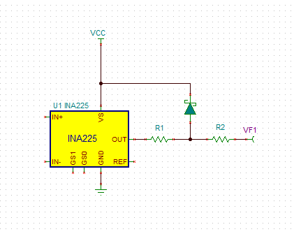
    If there's no other way to solve the problem, I would try to clamp the output voltage with a Schottky diode to the positive supply voltage, like shown here:

    R2 limits the current through the Schottky diode and into the supply line. Eventually a TVS is needed from the supply line to GND to provide a current path for the Schottky diode's current. The voltage drop across the Schottky diode should be below 0.3V.

    R1 not only limits the current into the output of INA225 but also decouples the output from the capacitive load of Schottky diode.

    Kai

  • Hello Koji,

    Thanks for your interest in the INA225. Yes, if your customer plans on having the output voltage exceed the recommended operating range and approach the absolute max voltage, we would advise to current limit to 5mA. Especially if there is a possibility that the voltage will exceed the absolute max.
  • Hi Kai-san Patrick-san

    Thank you for response.

    Is not it recommended similarly under the following conditions?

    VS = 14V
    REF = GND(0V)
    GS0 = GND(0V)
    GS1 = GND(0V) , 14V (Gain is two patterns of 25 and 50)
    IN+,IN- = No voltage applied

    Could you tell us the impedance between OUT pin and GND pin?

    Best Regards,
    Koji Hayashi
  • Hi Koji,

    the OUT pin is directly connected to the output of an OPAmp, so the impedance between the OUT pin and GND pin is very low ohmic. Figure 13 shows the output voltage swing versus output current. Also, internally of chip there are protection diodes connected from the OUT pin to the rails. That's why the output voltage must not exceed the rails by more than 0.3V.

    I haven't understood your first question. :-)

    Kai
  • Hi Kai-san

    Thank you for quick response.

    I'm sorry I didn't make it clear enough.
    I will rewrite the first question
    I described the status of other pins when applying voltage to the OUT pin up to Vs+0.3.
    Does it not change that a current limit is necessary ?

    Fig.13 is the result of VS = 5V, VREF = 2.5V, VIN+ = 12V.
    I think that impedance will change depending on conditions.
    Please tell me the impedance MIN/MAX in the following conditions.

    VS = 14V
    REF = GND(0V)
    GS0 = GND(0V)
    GS1 = GND(0V) , 14V (Gain is two patterns of 25 and 50)
    IN+,IN- = No voltage applied.

    If it is difficult, please tell me the MIN/MAX value under all conditions of design value.

    Best Regards,
    Koji Hayashi
  • Hi Koji,

    that the ouptut voltage pin must not be driven more than 0.3V above the rail is valid for all operating conditions. This is independent of supply voltage, input voltages and so on.

    An employee of TI must explain how the output saturation voltage at different supply voltages is. I don't have the manufacturing documents.

    Kai
  • Hello Koji,

    With respect to your opening question, I can say that overdriving output is not a good idea. This is because device impedance can be quite low, which you seem to be aware of. The output impedance for this device will be independent of supply voltage or common mode voltage as long as it is operated within the recommended operating conditions. However, the output impedance will vary with gain and bandwidth. Would you mind sharing what frequency signal you will be driving through the device and what you are trying to do on the output?
  • HI Patrick-san

    Thank you for response.

    IN+,IN- = No voltage applied
    No voltage is applied, I think that there is no frequency.

    Best Regards,
    Koji Hayashi
  • Hi Koji,

    but why do you want to apply a voltage to the output of an OPAmp?? This is most unusual. That's not what the chip is desgined for. You must connect an input of another device to the output of the INA225.

    Kai
  • Hello Koji,

    The internal output amplifier to the INA225 is the same as the output amplifier for the INA302. The output impedance for the 20V/V and 50V/V gain variants of the INA302 were measured to be under an 1 ohm for frequencies under 10kHz.

  • Hi Kai-san,Patrick-san

    Thank you for response.

    My customer apply voltage to OUT pin when only testing.

    I saw the INA302 data sheet, but I could not find a description that impedance is under an 1 ohm.
    Is this the result of INA302's EVM ?

    Best Regards,
    Koji Hayashi
  • Hello Koji,

    The INA302 is an older device and including output impedance was not a standard practice at that time. However, we have since then taken measurements, but have yet to post those test results in the datasheet. Would you mind sharing why your customer is testing this?
  • Hi Patrick-san

    Thank you for response.

    My customer is applying for failure mode test.

    Best Regards,
    Koji Hayashi