This thread has been locked.

If you have a related question, please click the "Ask a related question" button in the top right corner. The newly created question will be automatically linked to this question.

[FAQ] INA199: Does power sequencing for my current shunt monitor matter?

Part Number: INA199

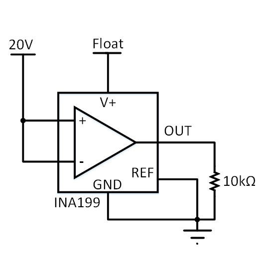
I expect that when I turn on my system, there will be a delay between when my microcontroller is ready for measurement and when my INA199
is properly powered on. Will this produce errors in my microcontroller readings?

  • Current sense amplifiers and power monitors have a significant benefit over other amplifiers in that the voltage rail from which current is measured can exceed the voltage source that powers the device.  There rarely are data sheet requirements for current sense amplifier products that dictate a supply power-up sequence, and in general, these products should be ok (not necessarily operational, but also not suffering damage) in the presence of one supply and absence of the other

    However, it is important to note that during power-up and under certain conditions where inputs or outputs are not biased or loaded, the behavior of the part is not specified and often not characterized.  Care should be taken during circuit design to account for unspecified behaviors, be that ignoring the output of the amplifier when the supply is floating, or perhaps including a pull-down resistor on the output to help keep the output from floating up.

    Various devices incorporated in a system may require a specific power up sequence to preserve their structure and ensure proper operation.  Such device requirements can add complexity and cost to a system.  Some reasons for providing proper sequencing include latch-up prevention and generating an expected output.  Texas Instruments current shunt monitors are designed to be robust and resistant to latch-up.  However, when a common mode voltage is applied to the sense pins while the supply pin does not have a proper operating voltage, offsets and atypical transient behavior may be observed on the output. Below is behavior that was observed for the INA199.

     INA199 with Floating Supply Pin Setup

    Figure 1: INA199 with Floating Supply Pin Setup

    Figure 2: INA199 Output When Supply Pin Floating

    The output observed on the output pin of the INA199 in Figure 2 was generated under the conditions illustrated in Figure 1.  From this figure we can see that without a supply voltage this particular device exhibits small periodic waveforms.   The above behavior can potentially cause problems if not accounted for during the design phase of a project.  The device will work correctly when biased, but while in the absence of its supply power it can potentially trigger a downstream device that takes various corrective actions that shutdown the system.

    For example, a device is disabled and then woken up periodically to make a measurement of current in a system, and shut down the system if the current exceeds some preset level.  This is a very typical application with a power saving method implemented.  Now, if the output of the device feeds an ADC on a microcontroller and the ADC makes conversions during the power-down time of the amplifier, the ADC could see a non-zero voltage.  If the microcontroller is not programmed to ignore the ADC measurements during amplifier power-down times, it could make a decision and take corrective action for a non-existent high-current condition.

    Aside from the output producing unexpected signals, the floating supply may also produce unexpected signals and thereby affect other devices using the same power rail.  Figure 3 shows how the supply rail for the INA199 is affected when using the same setup used in Figure 1.

    Figure 3: INA199 Output and Supply Pins When Supply Pin Floating

    From figure 3, voltage ripples approaching a standard rail value of 1.8V were observed on the floating supply pin.  If such behavior is a concern, one may simply ground the supply until power-up is convenient.  Often, for low power current sense amplifiers, this can be accomplished using a GPIO pin on a microcontroller to power and disable the device.  In this particular case with the INA199, the supply rail issue is fixed, but now the output exhibits different behavior.

    Figure 4: INA199 Setup with Grounded Supply Pin

    Figure 5: INA199 Output and Supply Pins When Supply Pin Grounded

    The behavior seen in Figure 5 was generated with the setup illustrated in Figure 4.  From this setup it can be seen that when the supply is tied to GND, the output presents a steady 600mV offset from ground.  Although a grounded supply pin can fix supply pin behavior, this measure may not even be necessary depending on the load of the output.  All of the above examples’ outputs have a 10MΩ load from the oscilloscope probe.  However, if the output load is changed to a sufficiently small value, the ripple on the supply will disappear.

    Figure 6: INA199 With 10kΩ Output Load Setup

    Figure 7: INA199 Output and Power Supply Signals when output load is 10kΩ

    The signals observed in Figure 7 were generated with the setup in Figure 6.  Here, the 10kΩ fixes the supply rail issue.  Also from Figure 7 it can be deduced that the load forms a voltage divider with the internal circuitry of the device and smaller loads ultimately result in more voltage dropping across the internal impedance thereby yielding a lower output voltage.  If the setup in Figure 6 is modified such that V+ is grounded, the results are identical.

    One last scenario of interest could be what kind of behavior the output pin and sense pins exhibit if only the supply pin is powered.  Figure 9 demonstrates the behavior of floating sense pins, while Figure 8 clarifies the setup.

    Figure 8: INA199 Floating Sense Pin Setup

    Figure 9: INA199 floating sense pins

    From Figure 8, some charge injects through some of the device parasitics creating a transient 300mV spike that occurs when the 5-V supply at V+ is turned on.  However, after this initial spike the output and input pins both measure near ground.  If the sense pins happen to be pulled down to GND, this behavior goes away as depicted in figures 10 and 11.

    Figure 10: INA199 Sense-Pin High-Side Setup

    Figure 11: INA199 Ouput and Input Pins with High-Side Input Setup

    FAQ content by Patrick Simmons. For additional questions, please use the e2e forums.
    TI makes no warranties and assumes no liability for applications assistance or customer product design. You are fully responsible for all design decisions and engineering with regard to your products, including decisions relating to application of TI products. By providing technical information, TI does not intend to offer or provide engineering services or advice concerning your designs.