This thread has been locked.

If you have a related question, please click the "Ask a related question" button in the top right corner. The newly created question will be automatically linked to this question.

INA240: Pspice PWM analysis

Guru 54077 points
Part Number: INA240
Other Parts Discussed in Thread: REF3333, TIDA-00909, , INA282

Is it possible to simulate the effect of  PWM duty cycle speed increasing output amplitude with full REF being added to the shunts current measurement? Transient analysis of a shunt (uV/A) is ok until the test bench speed of the PWM duty starts to overtake REF1+2 reference and incorrectly adding what seems is entire REF into the output magnitude. How can that attribute be evaluated in Tina or even stopped on test bench without adding a resistive output divider to ground?

Currently there are No 100n caps on each A1 REF1+2 which seems to increase output magnitude after omitting them from transient analysis, also on our test bench. It would seem 10uf placed on the +1.225v precision reference would be ample filtering alone. R2,R18 were (0R) and C12,C16 (100n) for the A2 test bench, produced the same excessive output amplitude as the PWM duty cycle increased beyond the actual shunt 500uv/A current measurement. Other words there should be less amplitude relative shunts 500uV/A * 20 gain producing only 10mV/A on INA output added to the REF floor of 1.224v. 

  • To your first question yes it is possible to simulate PWM duty cycles.

    It would appear your previous posted Tina model had the function generator with sweep time embedded from past analysis plots. Though the function generator was turned off it was somehow interjecting 12.5Khz PWM into IG1 which was latter added into the model as another PWM source was deleted. When function generator sweep mode was turned on with 300ms 100Hz-1MGhz IG1 source the A1 output was flat.

    As to your second more relevant question (REF1+2) it would seem there is an undocumented errata when pins are tied together and powered by an external precision reference. Exhibit A would include TIDA-00909 where REF2 was tied to ground for undisclosed reasons. That configuration is controversial relative to the engineers circuit analysis that seems to contradict external reference REF3333 sets INA output bias +1.65v. The bigger question that need be answered by TI engineering is how this REF1+2 differs with PWM duty cycle. Our case the A1/A2 artificially raising the output magnitude to include entire reference +1.225v in the output signal. Yet REF2 tied GND does not or did not in TIDA-00909?

    8.4.3.1 Output Set to External Reference Voltage
    Connecting both pins together and then to a reference voltage results in an output voltage equal to the reference
    voltage for the condition of shorted input pins or a 0-V differential input; this configuration is shown in Figure 28.
    The output voltage decreases below the reference voltage when the IN+ pin is negative relative to the IN– pin
    and increases when the IN+ pin is positive relative to the IN– pin. This technique is the most accurate way to
    bias the output to a precise voltage.

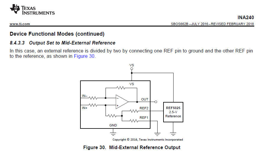
    Yet TIDA engineer only tested A1 with sinusoidal DSP wave form using the configuration shown below dividing external reference +1.65v in half. Yet that would according to other datasheet statements relative to INA output REF error % add even more error into the +/-16.5 amp window. Checking his math +1.65/2=825mV output bias, not +1.65 being inferred as the bias TIDA-00909 analysis table 2.


  • Our earlier finding 8 months ago was similar to REF1+2, when A2 output was set mid supply +1.65v. The A2 output had to be resistively divided 540mv or +1.65v REF caused excessive (overshoot) in SAR samples often tripping MCU embedded fault comparators.

    We ask for TI lab confirmation on why REF2 being tied to ground seems to control overshoot. When A1 output bias made 825mv per TIDA-00990 per Fig 30 or how REF1+2 causes undisclosed overshoot to occur. A workaround to stop overshoot of REF 1.225v into A1 output our Tina PWM transient analysis plots are not indicating a presence of any such occurance.
  • TINA models integrate collected data and design simulation data but are not perfect replicas of a device nor do they account for real world system differences like PCB layout or operating environment.  We understand that sometimes artifacts and responses not congruent to simulations are to be expected and that achieving robust design may be an iterative process.  In all of your threads (here, here, here, and more) regarding the performance of the device, we posit that the behavior you are observing is at a system level and likely the result of several factors outside of our part.  We strongly recommend you isolate the device from other possible sources of error both up or downstream of the device including the ADC and comparator with proper measurement techniques to minimize ground coupling so that you can evaluate the behavior of the device.

    With regards to your inquiry regarding both REF1 and REF2 being tied to an external precision reference, I did that test here.  The results of that test are that there was some noise on my lines, but the 12.5kHz PWM signals were amplified by a gain within the tolerance specified in the datasheet. With regards to your suggestion that TIDA-00909 will exhibit different behavior with an external reference, that design is available here at http://www.ti.com/tool/boostxl-3phganinv and I encourage you to try it out and possibly use it as a reference to evaluate against your system.

    If you believe you have received out-of-spec, defective or damaged parts, TI's customer return policy is here: https://www.ti.com/support-quality/resources/customer-returns.html

  • Patrick,

    I think you are missing the point and the evidence posted here in this thread which indicates the datasheet is misleading in factual content.

    That is to say the INA series we have tested with a PWM signal are not producing the correct resulting output relative to REF inputs level disclosers in datasheet. It is expected the REF threshold (bias) voltage is not to be added into the output of the amplifier as gain or any other artifact. You will notice from captures posted no matter REF1/2 bias level the output is always producing the same resulting amplitude near full scale ADC for what ever reason CMM/PWM rejection or other undocumented anomaly/errata.

    We have also tested single PCB versions of the INA240 mounted above low side shunts, isolated from the inverter PCB. The same output condition results no matter REF bias is made midpoint or below VS. It would be a far stretch to say there is some kind of defect in A1 yet Tina analysis is not producing similar plotted transient results. Tina transient models of the A1/A2 never indicate the output being near full ADC scale no matter what the RC filter design or shunt CMMV level. Likewise even harder to believe is 500uohm shunt producing +/-IN amplitudes the PWM rejection seems to pass right into the output gain. If it was an intent to lead customers astray by stating PWM rejection reduces shunt transients or CMM pass through within a datasheet disclosure (all uses of the product), that has been achieved.

    How the INA datasheet differs from real world test results derived from stated facts/miss facts in a datasheet is not for the customer to discover. It would seem from our forced investigation, datasheet disclosure developed relative to CMM/REF behavior is not completely without error thus miss representing functionality in key areas; 1 full scale ADC measures, 2 VS pin voltage levels relative to said full scale ADC. It would seem the datasheet used ADC to infer >3v3 full scale and A1 is not (fully) compatible with CMMV for all known types of PWM signals. Testing A1 transient response via sinusoidal DSP wave forms (TIDA-00909) hides facts of CMM/PWM rejection to benefit all use cases of the product revealed in sub context of this thread. The word PWM does not infer sinusoidal wave forms have explicit commonality to disclosed datasheet shunt PWM rejection or any other CMMV rejection which escapes any use clause being properly disclosed.

  • Hi Patrick,

    Below photos of previous test layout confirm our new custom PCB layout has nothing to do with why the output amplitude always peaks up to 2.7v @8amps , no matter REF bias level  VS=3v3. Other thread scope captures indicate 8 amps phase current inside a 75 amp or more ADC full scale (3.1v),  A1 or A2 devices via same 500uohm shunt value.

    There is something wrong with the use case of the INA in 3v3 ADC full scale measures that require proper datasheet lab disclosures. Simply put if the INA under certain low side conditions requires special handling of output relative to PWM signal types that must be disclosed in datasheet. We too in these photos were unaware the REF had little to no effect on the output typically nearing ADC full scale.  INA output signal required special handling even when set (1.65v mid supply) going well beyond datasheet text to imply PWM rejection solves all use case issues and typical CMMV noise types. Point is if the output amplitude must be divided for SAR 3v3 ADC full scale under certain CMMV noise types the datasheet leaves a donut hole for customer to fall victim to.

    As you can see the sub PCB (single) sits above 500uohm shunts and away from any noise source. Also note the shunt GND sources trough VIA to ground plane, each phase output never crosses any point of the CMMV inputs.

    What these several threads reveal is the INA is not rejecting certain type low side PWM signals, perhaps even passing them straight through to the output. That is for TI lab to properly disclose in the datasheet, not the customer to fall a victim of. We did our research but it appears TI has not even bothered to verify INA product suitability for certain PWM applications.

    Single INA240A2 mounted 2 sided jiffy PCB. 

  • Hello BP101,

    I assure you there are no intentional omissions from our data sheet.  Our characterizations are substantial and thorough but we cannot predict every way in which a customer will implement a device so your exact circumstance may not be covered.  We are happy to help you debug your unique circuit and layout as best we can and offer suggestions and opinions on what to try.  The boards you are showing photos of here appear to be in pretty bad shape and I wouldn’t be surprised if that is contributing to the issues seen in the numerous posted scope shots.  If I am misunderstanding these photos, please accept my apologies and it would be helpful to share photos of your good, clean setup that is undergoing testing.

  • Had you bothered to read photo text caption (prototype) used to study INA240 for later custom PCB we now employ.
    That layout PM to you directly counters idea you formed somehow custom PCB output signal crossing underside of ground causing peak transients is a mute point. Again shuts in photo do not cross the signal yet similar transients were present in that A1 output signal. Once again proves 240 PWM transient rejection is working as marketing fluff around 240 operation disclosure.

    This couldn't possibly be issues of datasheet omitting certain facts the Tina model then reversed in the process.
  • If the A1 and A2 device both show the same behavior, then I would suggest the layout contribution is significant. Please share the layout guideline we offered that you based your design on and your layout (annotated) so that we can review them.
    As we have said many times before, the TINA model is an approximation of device behavior. Also, it would appear that you are going back and editing some of your responses and removing information, making it difficult for us to refer back to it and better support you and people in the future. Please refrain from deleting content in your posts in these threads to maintain the integrity of the forum to help us help you and others.
  • Patrick Simmons said:
    Please share the layout guideline we offered that you based your design on and your layout (annotated) so that we can review them.

    How about you do your own research, the datasheet figure 39 was given. The device layout was provided in PM what more do you want.

    Patrick Simmons said:
    . Also, it would appear that you are going back and editing some of your responses and removing information, making it difficult for us to refer back to it and better support you and people in the future.

    Bashing user posted content in an effort to discredit content use without having a single fact to base that opinion is pure conjecture!

    Steering a conversation to fit your beliefs of intent for said posted content in an effort to redirect the topic is a bit cynical. There is a learning curve on both ends of this connection!   

  • Patrick Simmons said:
    As we have said many times before, the TINA model is an approximation of device behavior. Also, it would appear that you are going back and editing some of your responses and removing information, making it difficult for us to refer back to it and better support you and people in the future.

    8.4.3.1 Output Set to External Reference Voltage
    Connecting both pins together and then to a reference voltage results in an output voltage equal to the reference
    voltage for the condition of shorted input pins or a 0-V differential input; this configuration is shown in Figure 28.
    The output voltage decreases below the reference voltage when the IN+ pin is negative relative to the IN– pin
    and increases when the IN+ pin is positive relative to the IN– pin. This technique is the most accurate way to
    bias the output to a precise voltage.

    However the bench model behaves opposite of above datasheet 8.4.3.1 and Tina analysis is more complex than you give it credit but it too is not indicating the output behavior bench 240 produces. Laboratory analysis only includes VS=5v, VCM=12v (high side) and omits any data for VS=3v3, VCM=0v let alone provide a CUT diagram to explain typical bypass caps used to produce those test results. Sloppy laboratory analysis is no excuse to point fingers for customer use of device in Typical and previous disclosed TI marketing use of a device family.

    *****************************************************************************
    * Notes:
    * The model reflects the following parameters:
    * Common-mode input range, CMRR, VOS, IIB, Gain, BW, Vout versus Iout,
    * slew rate, noise, power supply range, IQ.
    * The model does not track device behavior over temperature

    *****************************************************************************

  • Patrick Simmons said:
    If the A1 and A2 device both show the same behavior, then I would suggest the layout contribution is significant

    This again is an attempt to discredit our 8 months device testing and instead replace it with an unproven opinion. It becomes oddly clear when reversing the Tina model +/-IN pins the signal behaves much as the bench A1 output would be expected to relative to 8.4.3.1. Yet INA240 pins 2,3 produce an opposite output polarity in the INA282, though depicted exactly the same inputs into the differential amplifier.

    We are witnessing REF1+2 pins doing the exact opposite on bench from that of Tina A1/A2 macros, perhaps based on incorrect data. This forum previously reported an inconsistent output behavior between theses two INA devices relative to similar datasheet figures. That report relates an unknown output inversion is occurring in the A1/A2 devices, yet no follow up occurred on behalf of TI. If keeping consistent behavior for shunt input connections to all INA devices is not important we have all been bamboozled.

    FYI: Figures 21,22 both do not indicate shunt orientation to +/-IN pins and only tested VCM, CMV=+12v. In reality when VCM/CMV<50mv the transient response is opposite to that depicted in Figures 21,22, again no real analysis of the device at VS=3v3. Please do not lecture on redacting or editing content only being used to prove a point thus being ignored is an attempt to discredit relative real testing the laboratory did not do at all.