This thread has been locked.

If you have a related question, please click the "Ask a related question" button in the top right corner. The newly created question will be automatically linked to this question.

INA213: Output Voltage reading is not the full reference voltage range

Part Number: INA213

Hello,

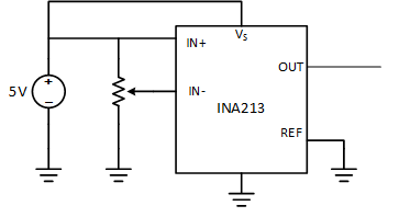
I am trying to use the INA213 to monitor current coming in from the power supply. As a preliminary step I am testing the device alone to find its capabilities. Below are my configurations. With this setup, I am increasing and decreasing the load and it seems that the output pin on the device is maxed out around 1V. I am looking for the understand why it will not output more than that. Ideally I would like it to span the VREF of the microchip which is 3.3 V.

Current sense Amplifier:

Reference: Grounded

V+: 5V

IN+: 5V

IN-: Load Potentiometer

  • Hello Justin,

    Thanks for your considering to use Texas Instruments in your system.  If I understand correctly your setup looks like the figure below.  As your supply is 5V, I would expect the max output to be 5V-0.05V = 4.95V.  This would be according to the the Swing to V+ power-supply rail specification in the electrical characteristics table of the datasheet.  As your output is far from that, your device could be damaged or you may have overlooked something in your setup.  Have you checked to see that all of your ground nodes are tied together?  If one of the ground nodes is floating you could get some peculiar results.  Is there anything else besides an oscilloscope or DMM on the output?  If there is, that may be dragging the output low.  Have you checked the current your supply is sourcing?  Perhaps if your potentiometer is really small, your source may not be able to provide sufficient current if you set the current limit too low.  If your potentiometer is large and you are hitting the current limit, you may want to disconnect the supply from the input pins (IN+ and IN-) and see what the quiescent current is.  If the quiescent current is over 100uA, then the part is damaged.  Are you using version A of this device?  If you are, its possible that the device could be damaged at power up.   Version A is susceptible to large fast transient signals.  Typically a power supply has a very slow ascent to the preset supply voltage, while a battery can dump charge and provide the desired voltage instantly in comparison.  The fast slew in voltage from the battery on the input pins could potentially cause latch-up with the internal ESD structure of Version A.  Consequently, we strongly recommend using INA213B or INA213C.

  • Thank you for all your input.

    As a follow up, the device being used is the INA213B, all of the ground nodes are tied together and there was an ADC connected to the output but that was removed.

    Originally the load was only a potentiometer which was not able to stand the power. This fixed the issue of the 1V reading. The reading is now above and beyond 3.3V.

    The quiescent current was then measured on 4 different chips. One of them read 114 uA while the other three read 96 uA.

    At this point the gain is very far off. For the INA213 the gain should be 50V/V, but it is around 300 V/V. This is consistent between all 4 chips I tested.

    Thank you in advance.

  • Hello Justin,

    The fact that one of these has a quiescent current above our specified max, makes me think that all of these devices may be slightly damaged. I suspect one of the absolute maximum specifications was exceeded. Could you keep the ADC disconnected, replace the current INA213s with new ones, and monitor the inputs, supply, and output at startup? Be sure to give me a scope shot if you observe anything peculiar.
  • On two brand new chips right out of the sleeve, the quiescent current was 88 uA and 160 uA. To clarify and make sure I am measuring the quiescent current the correct way, I am measuring the current in from the DC power supply to the V+ pin, in my case I am inputting 5V. I have also grounded the reference pin and left everything else (IN+ and IN-) open.

    Thank you

  • Hello Justin,

    You probably just omitted this, but be sure to ground the ground pin and then short IN+ and IN- together. If these are still high, that is peculiar. Are you testing your setup in an ESD controlled environment?
  • Yes, the ground pin is grounded, I did jumper IN+ and IN- as well. The test setup is also in an ESD environment.
  • Hello Justin,

    That is strange that you would be getting measurements outside of our specifications. As such I will run some tests on my end concerning the quiescent current as well as the load current. I will see if I can determine what is giving you those results and propose a workaround if necessary. However, this may take a day or so to do.
  • Is it possible that the resistors are damaged? The gain between all 6 tested devices is consistently about 300. Is it possible the devices were assembled with the wrong resistors?

    Please let me know if your tests show any similar results.
  • Hello Justin,

    Are you asking about the internal device resistors?  That is unlikely. We test our parts before shipping them out.

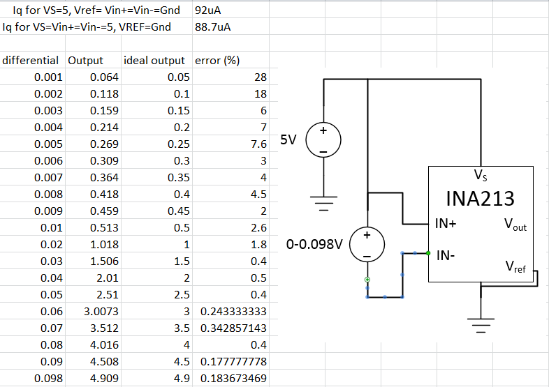
    Below are the results I got for the quiescent current and the measurements I got for various differential voltages across the input pins.   For my test I was able to get an output above 1V.

  • Is the circuit you tested a simulation? If it is not a simulation could you go into more detail about the "0-0.098 V" supply? Was a voltage supply used or current sense resistor and load? If a voltage supply was used was the negative terminal ground?

    Thank you.

  • Hello Justin,

    This circuit was done with our EVM. The 0-0.098V was used for emulating a voltage developed from current across a shunt. The input differential supply was floating in relation to the supply to the part. As such the negative terminal for the input differential voltage was not grounded.

  • I have set up similar tests and did receive the same results. In the mean time, I have also found that the resistance of the wires going to and from the shunt resistor was adding impedance. So the shunt resistor marking was 0.01 but the actual resistance seen from the wires caused the "shunt resistor" to be nearly 0.09 ohms. Obviously a large difference when it comes down to the calculations. I think this has solved our problem and should be easy to eliminate when done on a PCB.

    Thank you for all the help,

    Justin

  • Hello Justin,

    Glad to be of service. If you run into any further issues, please let us know below or open a new thread. Good luck on the rest of your system development!