This thread has been locked.

If you have a related question, please click the "Ask a related question" button in the top right corner. The newly created question will be automatically linked to this question.

INA240: Output inversion

Guru 54057 points
Part Number: INA240
Other Parts Discussed in Thread: TM4C1294NCPDT, UCC27714, EK-TM4C1294XL, INA282

Hello again,

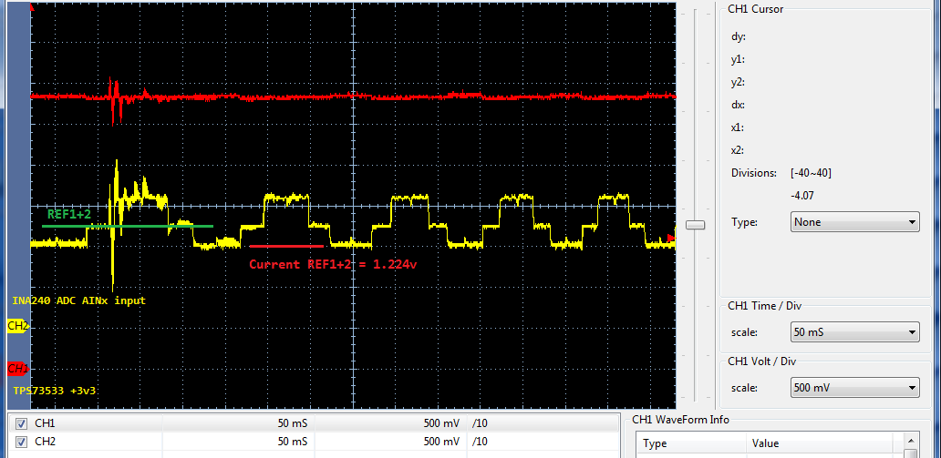
Many captures posted A1/A2 signals we of late see output inversion occurring unrelated to REF1+2 pins configuration.

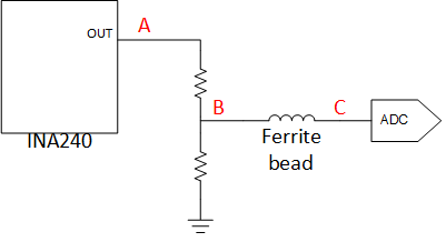
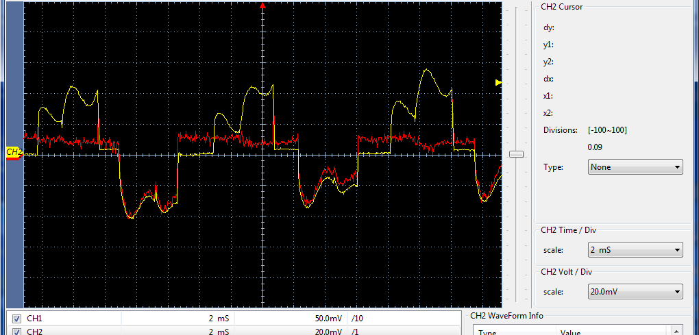
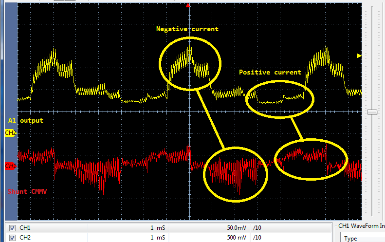
Basically the inverted output produces inverted peaks meant for mid negative REF. The output solution (A1/A2) seemingly produces inverse shunt or negative current on top and positive current on the bottom just above +1.224 REF1+2 rail. Otherwise the REF should divide the output signal mid supply of REF +1.224v when VS=3v34.

The A1 +IN pin faces +VCM source (from low side perspective) and -IN pin connects to GND. Datasheet suggests REF1+2 or 1/2 REF precision reference does not invert shunt CMV or +IN entering the non-inverting amplifier input. The 240 datasheet REF disclosure text mirrors 282 datasheet REF disclosure text, yet 240 inputs act opposite of 282 relative to REF configuration. So it would seem as the A1 output is then RC filtered the output inversion of shunt input signal widens above REF as below capture shows. Reported similar A1 behavior this forum was never acted upon by TI engineering to later include datasheet updates and proper CUT showing any laboratory testing of REF for all voltages in the VS range 2v7-5v5. 

CH2 represent PWM cycle by cycle measures (note) ride above REF relative to shunt input polarity meant for mid supply, not to be added to REF. Perhaps the datasheet incorrectly characterized REF pin behavior as it relates to VS=3v3 and or REF1+2=1.224v?  Otherwise REF pin violates datasheet specifications in the absence of REF pin testing below CMV+12, VS+5. 

  • Resized above pictures 4 times to fit side by side in web frame, via post edit. Yet the same post with extensively long frame is produced exact same fat pictures. Closed web browser, again same 4 appear after yet another edit of very same pictures sizes. Effort to keep threads short one must omit redundant or non important text, resize very wide pictures too.

  • Hello BP101,

    Can you clarify if your output measurement is at A, B, or C on the diagram below?

    We are looking into adapting some low-side sensing boards we had for another device to fit our INA240 and investigate your claims.  When I have more details on that plan, I will let you know.  In the mean time though, I would like to confirm your operating conditions:

    INA240 supply = 3.3V

    REF1=REF2=1.225

    Imax = 75A

    System supply = 79V

    PWM frequency = 12.5KHz

    VCM: low-side sensing ~=0V

    What duty cycle or range of duty cycles are you using?

    If you disable the inverter gate switching and keep the ADC on, what does your INA240 output look like?  Can you provide a scope shot of this?

  • Hi Patrick,

    Oddly it doesn't seem to matter where the scope probe is placed ABC as pluses are above mid supply. Multi layer MMZB102C ferrite or SMT 10uH Choke similar output ramping occurs. Resistively dividing output 4R87K to GND REF=620mv avoiding comparator fault tripping of output mid REF 1.224v and adversely creates random secondary over current fault conditions from rescaled transients.  

    Yet the ferrite seems to clamp faulting transients the choke lets through. All the values you posted seem accurate, PWM duty cycle 0-20% being steady state current is below 10 amps. Each PWM period 12.5Khz=80us with roughly 15-20us on time during steady state speed so duty cycles 15-20%  around PI speed controller.

    Capture below we see A1 output goes positive as the shunt voltage drops, very troubling. Tina plots without SAR in analysis indicate the output voltage dropping relative to initial shunt CMMV set @20mV or 80mV to match A1 bench results. If the SAR is causing the output to rise it would seem the INA low impedance output is not fully compatible. The SAR Rs via Cext now at (22nf) keeps analog impedance roughly 570 ohms.  See table 1 SPNA118B–September 2011 explains our filter selection (Cext=10n-22n) for 1/2 LSB of TM4C1294NCPDT MCU embedded ADC 12bit/16chan SAR Csamp=10nf @2MSPS.

    Capture of first motor run, shunt CMMV drops yet output jumps far above REF. CH1 probe 10x, channel 1x not exact scaling but seemingly much closer to reality of Ohm's law E=IR 500uohm. The capture indicate roughly +/-8mA up to +/-2.2 amps

  • Patrick Simmons said:
    If you disable the inverter gate switching and keep the ADC on, what does your INA240 output look like?  Can you provide a scope shot of this?

    The capture above and a few others show exactly that as the UCC27714 gate driver outputs are disabled until the PWM drive is 1st applied. The ADC is always running measuring bus voltage and other sensors, current samples occur 1.25us after PWM drive though A1 outputs are always active into SAR channels. There is little chance of cross talk as defined (SPNA118BSeptember 2011). The A1 three SAR channels are in line, isolated from other analog signals and show no indication of cross talking on the Cext filtered signals. Ideally larger values of Cext keep the SAR input impedance low relative to higher Rs values.  

    Seemingly the same A2 inversion problem with EK-TM4C129XL and proto testing 240.Prior to custom PCB we put a patch on issue dividing output from REF set mid supply (1.65v) not fully comprehending A2 output signal behavior relative to shunt CMMV changes.

  • The system supply was 165vdc with EK-TM4C1294XL proto inverter, 240 output resistively divided 540mv from REF1/2 set mid 3v3 supply.

    Currently power supply remains 80vdc (linear) until 240 issue is resolved. Also 24v (linear) bucks to +5v via 1.5Mhz Rohm switcher regulator feeds 3v3 LDO for 240 VS pins.

  • Requested scope shot sampling A1 outputs. CH1 scale is low as it can be set and suspect 80 VDC supply noise. CH2 level shows A1 output resistively divided half REF (620mv) sampled @1ms intervals of 80us PWM periods. 

  • Hi Patrick,

    Again the problem with 240 is the output is not splitting the +/-IN to mid REF and the output signal rides REF to rail. Datasheet  VCM specification -4v to 80v is part of PWM rejection filtering of output for REF split mid supply or 1/2 REF (1.224v). Figure 21/22 show VCM input signal (differential probe?) depicted above ground and refers the output at TA = 25°C, VS = 5 V, VCM = 12 V, and VREF = VS / 2 (unless otherwise noted)

    It would seem 240 output is not bipolar with respect to VCM of the PWM current measure and only produces reverse VCM below mid supply! That behavior is not linear ratio metric as it relates to the current being forward (positive) with reversals (negative) respect to REF=VS/2.

    We later attempted to filter out the non active PWM reverse currents that were not part of PWM inductive current cycles, thus were left with a non-ratio metric VCM 240 output. The NFET body diodes of 1/2 bridge control move current even when the low side NFET is not actively switched on. That is part of PWM synchronous rectification and not part of active inductive phase current measures the 240 must produce inside 3v3 SAR full scale window. Software knows when to sample active PWM inductive current but can not fix the incorrect VCM behavior of A1 output. 

    This capture shows the wave form that should typically be produced at all PWM duty cycles. Sadly only does for short time at very low duty %, output CH2 should be (noted +1.224v REF1+2 / 2). This behavior makes 282/240 unsuitable for MCU +3v3 SAR use in low side large value full scale current measures >20 amps with any precision. Seemingly pitfall skirted by INA series monitors not maintaining consistent VCM/REF behavior for 3v3 SAR compatibility in >30A full ADC scale current measures?


  • Shunt VCM not being split mid supply REF seems to counter points made in datasheet shunt VCM being equally divided in REF set bias. That is not necessarily a bad thing if the same signal pattern or similar above last capture results from REF1,2=GND. Datasheet text argues point bidirectional VCM is not possible REF1,2=GND. Yet how would current reversals then occur in bipolar inverters if not from a valance level (near GND) into B+. Clearly the capture above shows VCM current reversals occurring REF1+2=+1.224v. The larger peaks above REF shown in first post capture are perhaps faster PWM period reverse currents (below VCM ground) and inverted are due to switch noise or Delta V/t?

    The idea that VCM current reversals below ground later being summed with reverse currents and being inverted above split REF makes the full scale VCM difficult to manage @20v/v gain, even more so @50v/v gain. The minimal filtered output (Cext=200pf to 1n) seems to keep VCM reversals split REF of faster PWM duty cycles but the 2MSPS SAR can not make sense of the signal without output magnitude being extensively divided down or extensively filtered. The problem is the result is not the real and slower DC motor phase current, it (solution) is mostly the periodic PWM reverse current.

  • Hello BP101,

    So we now ran a test with the INA240 on a low-side motor drive board.  Unfortunately it is not readily feasible to re-adapt this current design to match your specifications.  However, it still can illustrate that this device can properly follow the sense voltage without inverting the output.  The board we used in our setup is low-side.  The bus voltage for our inverter is 20V.  The phase period is about 50us at a frequency of roughly 20kHz. The duty cycle was 86%.  Our supply was at 3.3V and the REF (blue-trace) was externally set to 1.65V.   In our tests we did not bother to band-limit the probe inputs on the oscilloscope.  From this you can see that our shunt measurement is quite noisy (violet-trace).  However, our output (yellow-trace) is rather clean in comparison.  We do have some spikes on the output.  Those are from the ground bounce.

  • Hi Patrick,

    Thank you for the effort (A+) yet sadly such benign testing is futile in light of the evidence being reported in this post and others.

    Patrick Simmons said:
    The phase period is about 50us at a frequency of roughly 20kHz

    Noted sine wave producing  (complementary paired PWM signals) CMV +/-IN does not produce the same output signal as trapezoidal waveforms.

    Patrick Simmons said:
    From this you can see that our shunt measurement is quite noisy (violet-trace).

    Shunt R3 seems to be missing from PCB so the long wires add much capacitance into PCB filter resistors R8,9,1,2 that should not even be present on the 240 test PCB. Datasheet hypocrisy in the text stating PWM rejection filtering precision is effected by external added filtering and discourages the use of any such filtering! It is not an engineers design requirement to correct device errata especially from undisclosed device behavior not being provided in the datasheet.

    Datasheet claim of PWM rejection filtering does lead to poor device performance without external shunt filtering being added as your experiment seems to prove. Excessive shunt noise appears to drive 240 output above split or REF 1.224v due to rapid current reversals, e.g. not present in sinusoidal wave forms, e.g. Complementary A/B PWM signals.  The inductive current of trapezoidal wave forms has more rapid current reversals than a sinusoidal wave form. Seemingly the slower DC current of trapezoidal wave forms behaves differently output bias set mid VS or directly from REF as it has been defined in datasheet.

    Your test compares apples to oranges and basically proves none of what was posted this thread. Seems you are attempting to change the narrative by even posting results of dissimilar wave forms. All you proved is the datasheet has not provided proper testing of the 240 with several types of PWM signals. TI now seems to consider valid PWM waveform being only (sinusoidal) exempting all others from the equation?

    Results from our evaluation of 240 it is very apparent TI used only complementary paired PWM signals producing sinusoidal wave forms in laboratory testing relative to PWM rejection claim and completely ignored other PWM wave types. Therefore there are no warnings that input filtering is specifically required with certain wave forms for PWM rejection to stop REF (errata) from occurring! Otherwise full scale current measures in excess of 30 amps remains unproven A1/A2 to produce any precision (VS=3v3, REF=VS/2) and claim >10mv shunt full scale measure is highly misleading statement when it struggles with 75 amp full scale @10mv/A with a simple trapezoidal wave form. 

    Otherwise the datasheet makes several unfounded claims of specific REF behavior to produce output bias levels and appears to cause output signal errata seemingly relative to certain decibel levels of shunt noise on +/-IN pins. if even biased below 1.65v or mid REF 1.225v for certain PWM wave forms CMV +/-IN pins the 240 device behavior is very certain of several bias perspectives as posted scope captures indicate some kind of REF errata is occurring in these captures regardless of external filtering issues

  • Patrick Simmons said:
    However, our output (yellow-trace) is rather clean in comparison.  We do have some spikes on the output.  Those are from the ground bounce.

    Perhaps what your missing is everyone of those yellow spikes in A2 output is delta V/t switch noise passing right on through PWM rejection filter.

    So we can not tell did your shunt (-) on PCB go to other PCB shunt ground,  what of (+) input low side FET source? 

    Do agree the PWM rejection does seem to clean up good part of the shunt noise though we are still capturing rolling cycles of flyback pulses well above scope vertical in that very same signal. Both A1,A2 and several inverter PCB what seems to be flyback pulses are getting right through PWM rejection (-93db) down. Luckily software low pas filters most of that out but only at certain duty cycles does that ever occur. Might you test that same flyback may occur on output from your sinusoidal test rig?

    So BLDC motors produce inductive flyback you will not capture occurring sinusoidal 120 degree motor commutation. The three motor phases are being active together at all times with sinusoidal. Again an apples to oranges comparison does not line up to our discovery of 240 REF behavior.

  • BP101 said:
    So we can not tell did your shunt (-) on PCB go to other PCB shunt ground,  what of (+) input low side FET source

    Patrick your scope capture (zoom) shows IN+ to GND and the yellow trace indicates reverse current flow into B+? Otherwise in forward current the shunt CMV +IN pin 2 potential rises above ground (positive) direction same as datasheet REF disclosure suggests for both 240 and 282. Both datasheet can not have the exact same REF disclosure regarding CMV polarity, if +/-IN is reversed relative to output signal polarity!

    The current probe capture below triggering 240 output signal indicates an 240 output inversion is occurring for positive current flow from shunt CMV. The NFET source (+IN) pin remains above ground potential in positive current flow. Accordingly datasheet REF disclosure states the very same conditions yet the 240 output is inverting in the capture below.

    How can that be unless the REF disclosure is incorrect for said pin diagram and inverted output. Main reason for the posting in forum 8 months ago asking why 282 +/-IN were backwards from 240 signal being inverted, not receiving a proper response from TI engineers. The REF1, REF2 pins behavior disclosure does not correlate with the 240 output signal behavior being opposite of positive current flow theory.  Shunt CMV +IN pin will have a higher potential than does -IN tied to ground for all forward current but 240 has randomly inverted the output

    If you are saying shunt (magenta) indicates current flowing to B+ then the output is inverted relative to REF disclosure, being -IN faces NFET source into supply B+. Your test rig would be detecting reverse current or electron flow into B+, negative current from a ground perspective. We past tested 240 +/-IN pin polarity reversal and did not get repeating ramp pulses in 80us periods for each 80us period cycle. Each 80us period produces inductive current flow or transient response of A1/A2 output. Retested 8-22-18: 240 +IN=GND and output does invert as shown below.

    CH2(yel)=Hantek CC65 clamp CH1(red)=A2 inverted output +IN=GND.


  • Patrick Simmons said:
    We do have some spikes on the output.  Those are from the ground bounce.

    Perhaps NFET high frequency RF (10-19Mhz) switch node noise, suspect causes some channel cross talk scope triggering circuit. Tektronix storage scope triggers seem to be less effected by RF, our Tenma 30Mhz even restricting BW 1000SPS deep does basically the same thing. 

    Against TEK 2430 storage scope signals pale yet CH1 is starting to fail after fully rebuilding the switching power supply 2015. 8" LED screen set 1 second persistence can not do what phosphor CRT did and does for best of human eye signal recognition. 

    INA282: REF12=GND, Shunt=9mohm, +IN=GND, otherwise +/-IN reversed no ratiometric 80us current ramp occurs as shown below.  


  • Looking at the shunt signal inverted CH1 the A1 output lines up to shunt CMV with a slight phase shift, scope trigger CH2. The 240 REF1+2 tied to ground should reduce output amplitude, if REF has any control over the non-inverting amplifier (+IN) open loop feedback gain. 

    Apparently there is very little change A1 output magnitude for forward current flow derived from shunt CMV or (+IN) potential technically rising above (-IN=GND) in current flowing to ground. Any rise in shunt CMV potential during forward current (B+ to GND)  and +IN being 1 resistor drop above ground (500uohm). Theory tells us +IN will rise above ground potential, not fall below it and only fall with B+ dropping several volts under motor load condition and again rising during DC recovery. 

    So the A1 output should not be inverted in that case yet it certainly appears it has been internally inverted via PWM rejection circuit or differential amplifier. Ideally PWM 80us or 50us periods should join to form a full ratiometric signature of those single PWM events as the captures above thus indicate typical both 282, 240. Yet occurs at an inverted and elevated output gain that defies amplifier gains shown INA240 datasheet. Perhaps there are limitations of 240 CMV and SAR full scale measures relative to monitor position not being disclosed in datasheet? 

    The capture inverted random CMV signal CH1 being phase shifted CH2 trigger source. Seemingly CH1 indicates large reverse current events being detected in opposition to +/-IN pin orientation and output CH2. Otherwise 240 not producing properly scaled ratiometric forward current signature required for SAR decoding 240 low side monitor? Instead we see CH2 floods SAR near full scale from only very small yet random CMV peaking events.

    Below was captured to show how CMV incorrectly is inverted by the non-inverting input. After all we want the A1/A2 output signal to keep fairly consistent with changing PWM duty cycles and produce signal closely resembles Hantek CC65 current clamp as being clamped to any single motor phase wire shown above posted capture. Reversing the 240 +/-IN pins does not accomplish any such signal behavior allowing SAR to preform a (scaled) decode to 1/2 LSB let alone 1/4 LSB.

    Are we fooled by 240 monitor position expecting similar results all PWM duty cycles that do occur only in low PWM duty cycles, (second capture) of well balanced PWM current even as it was being inverted above REF?