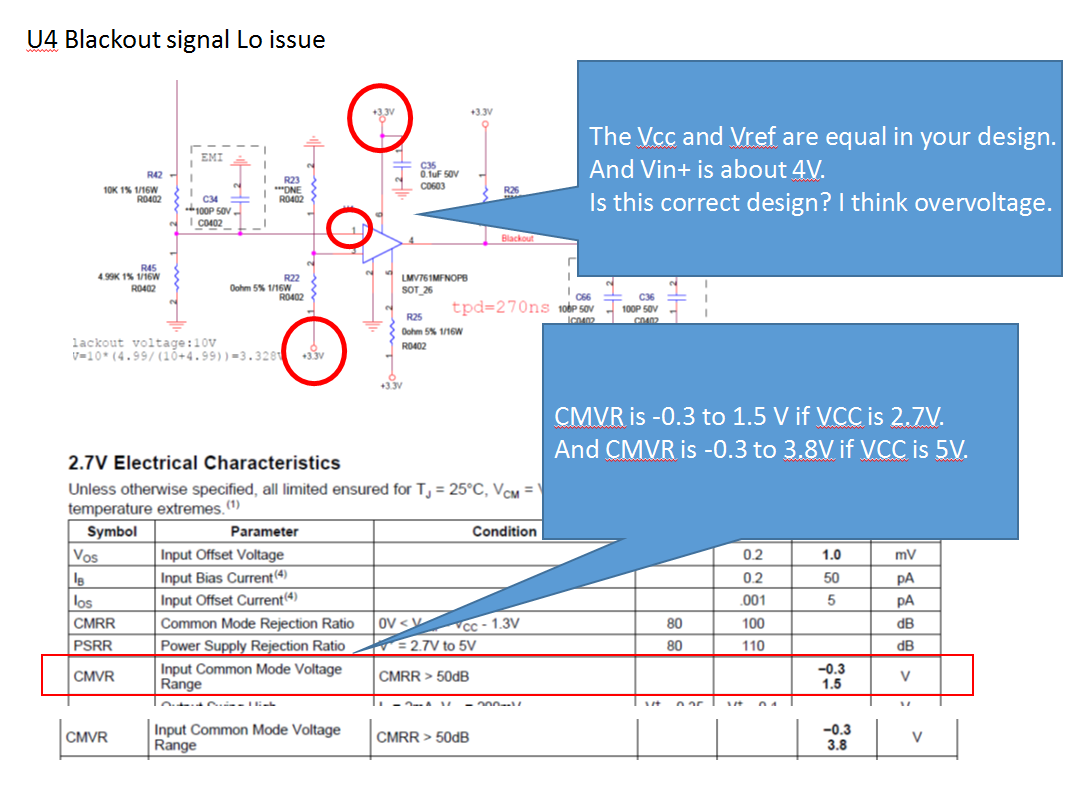
This thread has been locked.

If you have a related question, please click the "Ask a related question" button in the top right corner. The newly created question will be automatically linked to this question.

LMV761: Absolute Maximum Ratings Check

Part Number: LMV761

Dear E2E member,

I want to know the differential input which is IN+ - IN-,  the maximum rating is  5.5V, right?


Is it OK for this design as below?
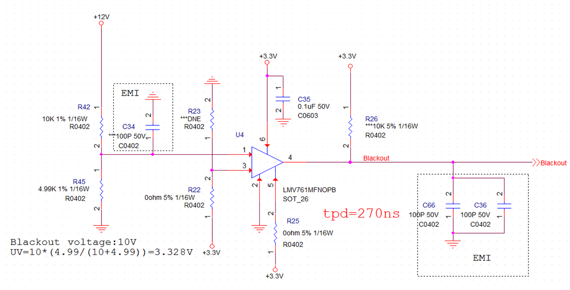
  • Hi Julian,

    looks good so far. But why have you mounted C36 and C66 to the output? The LMV761 toggles very fast at the output and toggling into a cap will generate a considerable load current spike. This can produce lots of noise on the supply line and signal ground.

    Kai
  • Dear Kai,

    Please refer the question as below,

    Customer means the CMVR just only -0.3V~3.8V@VCC=5V

    But the pin 1  of LMV761 is 3.9V, Pin 3 is 0V when 3.3V not ready.

    So Pin1 - Pin3 = 3.9V when   3.3V not ready.

    It's a risk for this design?  Does IC will abnormal at a moment when 3.3V not ready?

  • Hi Julian,

    is this the schematic you originally posted?

    Well, of course, the input voltages must not violate the common mode input voltage range! Change the voltage dividers so that the input voltages are allways within -0.3V...2.1V.

    And I would remove C36 and C66.

    Kai
  • Dear Kai,

    Thanks for you reply.

    I still want to confirm some questions.

    1. Now 3.9V sequece always prior than 3.3V. So What can we do in this design? Do we need to change others part?

    2. If over CMVR, what the issue does IC happened?

    3. What the CMVR SPEC at VCC=3.3V of LMV761?

    Thanks!

  • Hi Julian,

    Below are the answers to your questions:

    1. I would recommend that you change the power up sequence so that the device is powered up with 3.3V before signals are applied to the inputs. The ESD diodes will always be conducting otherwise and this is not expected use for ESD diodes of the device.

    2. Going over the CMVR of the device will lead to unexpected behavior and can also damage device. As I saw in the first screenshot you posted, you are seeing a propagation delay of 270ns which is double what it should be.

    3. The common mode voltage range of the device is from (Vee-0.3) to (VCC-1.2V). So in the case of 3.3V this would be from -0.3V to 2.1V.

    Regards,
    Jas
  • Hi Jas,

    Thanks for your reply.

    What will happen when signals are applied to the input before IC VCC is ready?

    In the current application, it's a bit hard to change power up sequence to meet your requirement.


    Gary

  • The input ESD diodes will be conducting every time the device powers up which is not their expected application. If there is no other option do you know what the input current is at the inputs when the signals are applied before VCC is ready? It should be kept to less than 1mA.

    Regards,
    Jaskaran
  • Dear Supporter,

    We'd like to add 3 capacitors to reduce input noise.

    Please help to review this circuit or provide your idea to reduce input noise.

    C34,C72 and C73:1000pF

    Gary


  • Hi Gary,

    looks much better now. :-)

    I would omit C72. C34 and C73 is enough filtering of inputs. And, as mentioned earlier, I would omit C36 and C66. The LMV761 toggles very fast at the output and toggling into a cap will generate considerable load current spikes. These can produce lots of noise on the supply line and signal ground. Be very careful with caps at the output of a fast comparator...

    Kai
  • Hi Kai,

    Got it.

    Thanks

    Gary