This thread has been locked.

If you have a related question, please click the "Ask a related question" button in the top right corner. The newly created question will be automatically linked to this question.

LMV842: Abnormal output for UV sensor application

Guru 19495 points
Part Number: LMV842

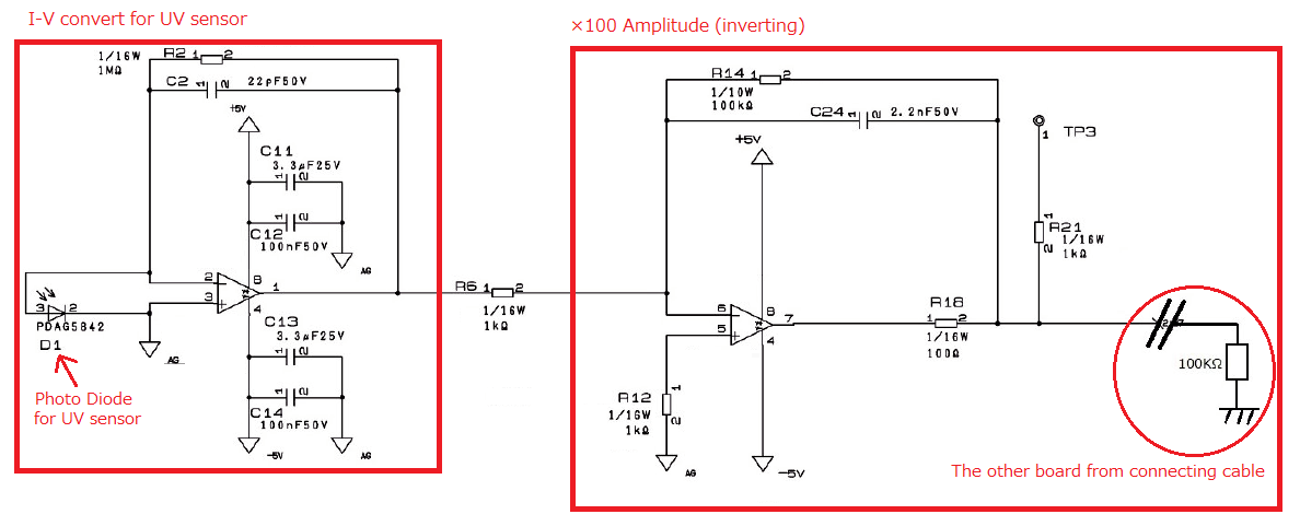
Customer is testing below circuit for UV sensor application.

Sometimes, this circuit is occur abnormal output.

⇒7pin output is near -3.2V~-3.5V, Test Pin 3(TP3) is -0.95V. 

If there correction point for below schematic, please let me know.

Best regards,

Satoshi

  • Satoshi-san,

    Your LMV842 circuit appears okay on the surface, but the dc output levels at pin 7 and TP3 should be about the same regardless of polarity. If both points are being measured with a very high input impedance DVM the addition of R21 in the TP3 path shouldn't result in any significant voltage drop. However, if the DVM resistance is lower than expected a voltage divider would be formed with R21 resulting in a higher voltage at pin 7, than at TP3. 

    The output voltage of the first stage, the transimpedance stage, will be driven to a negative voltage as the photodiode current increases. However, since the second stage is an inverting voltage amplifier stage its output would move to a positive voltage when a negative voltage is applied at its input. So if the photodiode is being excited by UV light Pin 7 and TP3 should be at a positive voltage level. Check the circuit wiring to make sure that everything is wired per the schematic.

    One last thing, check Pin 1, Pin 7 and TP3 with a wideband DSO. Make sure that nothing is oscillating. Oscillation can really mess up dc measurements.

    Regards, Thomas

    Precision Amplifiers Applications Engineering