This thread has been locked.

If you have a related question, please click the "Ask a related question" button in the top right corner. The newly created question will be automatically linked to this question.

OPA2180: Large offset in inverting buffer circuit that is outside the expected 70uV spec for the device

Part Number: OPA2180

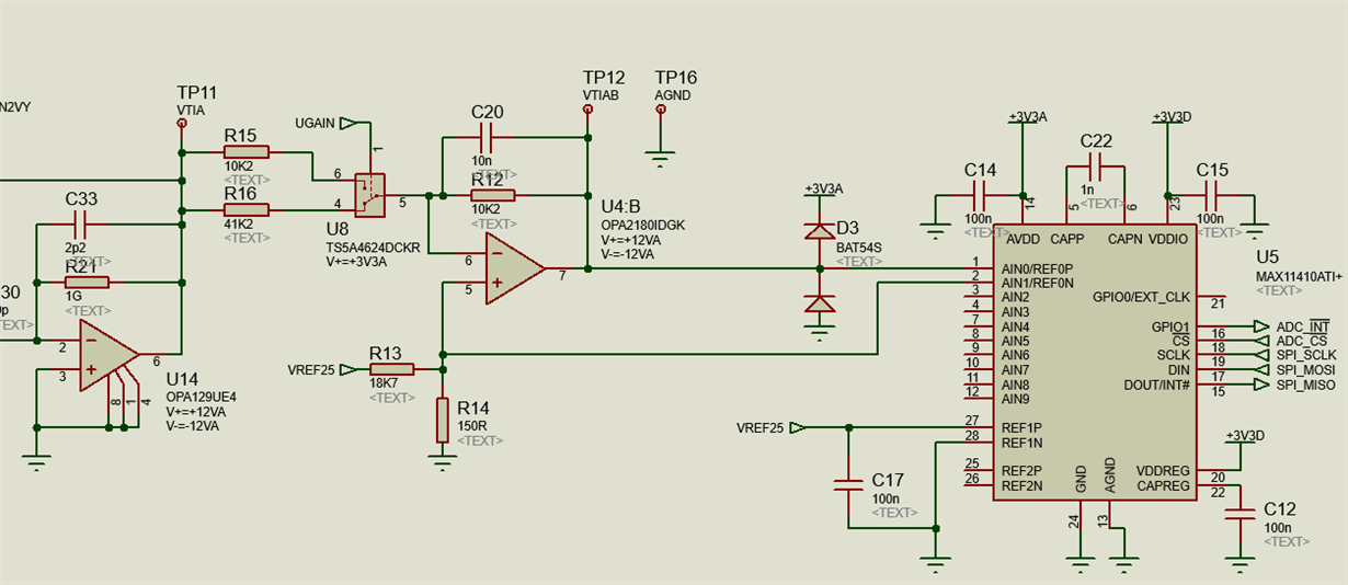
I'm using half of an OPA2180 to invert and add a small offset to the output of a transimpedance amplifier. See circuit below. Signal from transimpedance amplifier is applied directly in place of VS2 (hereafter called, the input), and spans around 0 to -10V. Vout drives the next stage of the circuit, an ADC input.

At the non-inverting input, the resistor divider sets 19.9mV. So, I would expect the output to be (19.9mV +-75uV) * noise_gain, where the 75uV is the max. offset error for the OPA2180, and the noise gain is 1 + (10k2/41k2). I.e. output should be 24.8mV +/- 90uV or so depending on the offset voltage of the op-amp sample.

However, in the real circuit, under the same input conditions, I measure an output voltage of around 22.36mV, about 2.5mV less than expected.

I then shorted the 150 ohm divider resistor, such that now, both the input (VS2) and the non-inverting input were 0V. I expected the output to be the op-amp offset voltage, i.e. +/-75uV. Instead, I measured -3mV on the output. That seems to me as though the op-amp is exhibiting an offset voltage tens of times bigger than the expected 75uV. I did also try another sample of the op-amp, and got the same behaviour.

What am I missing?

  • Hi Ross,

    I believe you forgot to upload your schematic, but there are many other sources of offset that you are not considering, such as that produced by bias current flowing through large impedances, CMRR, PSRR, etc. You may find this article useful: Real Vos 2017.docx

    How are you measuring the output? If you are measuring this through the ADC than what you are likely seeing is actually settling error from sampling

  • Dear Zak,

    Thank you for your quick response, and appologies for the missing schematic, here it is. To answer your question, no, I measured node VTIAB using a DMM, not the ADC. In the meantime, I'll digest the info provided in your link.

    I should give a bit of background... One of my development tests for this circuit is to check that the offset at node VTIAB matches my design value. The circuit has two gains, switchable via U8.

    Adjusting the gain changes the noise gain, so each gain results in a different offset voltage at VTIAB. So, I do my test twice, once for each gain. For a gain of -1, when R15 and R12 are in play, the offset at node VTIAB matches my calculation precisely. However, when I set a gain of 0.248, when R16 and R12 are in play, I get the unexpected result detailed in my last message.

    To measure the offset I manipulate the current being fed to transimpedance amplifier U14 such that I have 0V +/- a few uV at node VTIA. Under this condition I excpected the voltage at node VTIAB to be as explained in my last message.

    On getting an unexpected result, I tried the following:

    1) Cut track between node VTIAB and ADC to remove ADC from equation, no change

    2) Remove analog switch U8, and just short pads pin 4 to 5, no change

    3) Swapped op-amp sample for another, no change

    4) Shorted R14, so that voltage at non-inverting input is 0V, which gave -3mV or so at node VTIAB. (I expected to see +/-90uV max. or so)

    5) Confirmed values of gain setting resistors were correct, by verifying that the signal gain was as expected.

    There must be a clue in the fact that set to a gain of 1, the circuit works as expected, but set to the alternate gain it does not, but I have not been able to work it out.

  • Appologies for the further confusion, but double checked and I get the same offset problem for both gains, not just the attenuate gain as I first stated.
  • Hi Ross,

    Have you tried looking at the output with an oscilloscope just to make sure there aren't any unexpected oscillations?

    Another useful test would be to increase the resistance of your gain setting resistors, to 100kOhms for example, while maintaining the same gain. Whether this impacts the magnitude of the offset will give us a better idea of what might be contributing to it.
  • Dear Zak,

    I found out what was causing the problem; I had fitted some BAT54 clamping diodes, on the inputs to the analog switch, not shown on my schematic because I'd added them on as a mod to the board to fix another issue. Leakage current from the diodes was affecting the amplifier. Once removed, everything checks out as it should. Discovered when I was doing some temperature testing of the board and found that the offset was exteremely temperature sensitive, and realised that the clamp diodes were to blame!

  • Hi Ross,

    I'm glad you solved the problem, and thanks for sharing! Let us know if there is anything else we can assist with.