This thread has been locked.

If you have a related question, please click the "Ask a related question" button in the top right corner. The newly created question will be automatically linked to this question.

INA139: Measurement delay after negative common mode voltage applied

Part Number: INA139
Other Parts Discussed in Thread: INA210, INA225, INA199, LMP8481, INA250, REF200

We are measuring high side current draw on a standard half-bridge, driving into an inductive load. Our design is using the INA139 as a current protection device to turn off the MOSFETs during a short circuit event. As such, we need to have a very fast measurement.

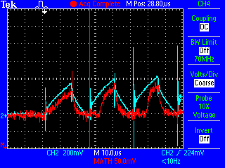
In a standard 50% duty cycle application, the inductive load is pushing the current back to the bus and biasing the input to the INA139 backwards. When the MOSFETs are turned back on, the INA139 takes up to 5us to start outputting it's measurement again. If the previous cycle doesn't push current back to the bus, then there is no delay.

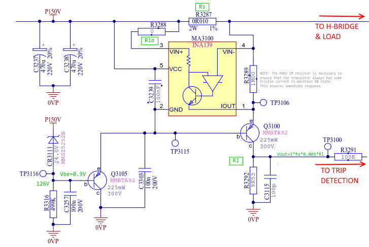
Our application isn't very different from the 'Bipolar Current Measurement' application shown in the datasheet, but we just don't care to measure the other direction.

Could you please explain what might be causing the delay, and how we can change our design to prevent it?

Thanks.

(RED is output @ TP3100)

(BLUE is AC current probe at the load)


  • Hello Stephen,

    I have been looking this over with my team and we have comments below.

    The  delay is not due to a negative common mode voltage, but a combination of the offset voltage (Vos) and IOUT saturation. The common mode voltage should be relatively stable at (Vin - GND) = 150V - 126.9V = 23.1 V.  However once there is inductive kickback, the differential voltage across Rs (Vsense) will definitely go to 0V and most likely below 0V. Once this happens you will saturate the IOUT pin, basically overdriving the internal amplifier's output stage to the GND level.

    Once the inductive kick back is over and the load current starts to rise, there will be an initial delay in the INA139 response as Vsense has to exceed the Vos of the part before anything on the ouput occurs. We spec the the Vos at +1.5mV maximum. After the the Vsense exceeds the Vos, then the output stage can start recharging to come out of its overdrive state and into its linear range of operation. The will contribute additional delay and most likely the majority of the delay.

    There are a couple options you can consider. One, you could bias the IOUT pin with a current source so that even if Vsense < 0, the IOUT pin is still in its linear region of operation. This is discussed in the INA139 datasheet as seen below. This should fix the delay since we do spec 2.5us settlings times for gain = 10 (RL=10kOm) and the Vsense is jumping from what looks to be 0V to 200mV (see below).

    This should fix the problem, but if not the other option is to use a voltage-output current sense amplifier part with a much lower Vos and reference the output to mid supply or something over its ground level so you don't have to worry about saturating the output. The following devices can support 25V power supplies and common mode inputs: INA210, LMP8481, INA199, INA225, INA250.

    If my assumptions about the design are incorrect or if you have more questions please post back to the forum.

    Sincerely,

    Peter Iliya

    Current Sensing Applications

  • Hi Peter,

    This is exactly what is happening, I am sure. Thanks for taking the time explain the results that I am seeing!

    -- Stephen

  • Hi Peter,

    I've taken over this project from Stephen (original poster). We took your advice and looked into eliminating the delay by adding a resistor to raise IOUT with respect to GND (Roffset, in pink, in the schematic below). It did help the delay significantly, but we weren't able to get it below about 2us. Is it possible to further eliminate the delay? We were expecting to see the delay get smaller as we raised the offset (we tried up to about 2V), but that was not the case.

    The chart below shows the results through a resistive load. We are trying to eliminate the delay we see on startup in certain cases. The black trace shows the original delay, and the green/orange/yellow traces show the responses with an offset resistance applied. We tried raising the offset to see if the delay would go away, but it didn’t go below 2us.

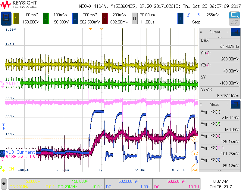
    Also below is the result through an inductive load with Roffset = 82kOhm, to compare with Stephen’s original image. We see some delay here too.

    Again, is it possible to further eliminate the delay? At a 2V offset we didn’t see much difference from 1V.

    Thanks for your help.

    Savitri

    Schematic:

    Resistive Load:

    (Black/green/orange/yellow is output @ TP3100 for different values of Roffset)

    (Blue is AC current probe at the load)

    Inductive Load:

    (Pink is output @ TP3100)

    (Blue is AC current probe at the load)


  • Hello Savitri,

    Is there any way I could get what the actual current values are for the resistive and inductive load plots you show? Or what the sense voltage is over time?

    We are looking into the circuit design now.

    Peter Iliya
    Current Sensing Applications
  • In both cases, I was driving 1A. The sensitivity of the AC current probe we're using is 2A/V (so the peak current for the resistive load is about 1A, same with the first peak in the inductive load plot). 

  • Thanks Savitri.

    There are a couple aspects to this circuit we are still trying to understand. You are measuring TP3100 with respect to ground correct? Is there any way you could use a differential probe to measure Voffset? This is the actual load the INA139 is driving and would provide us more helpful information.

    Also do you have any explanation as to why the zero current conditions for no Roffset vs. having Roffset are different? It makes sense that TP3100 is around 212mV since the 1MOhm Rbias is creating aout 25uA of trickle current, but adding Roffset of 82kOhm, should decrease this current by a negligble amount, making trickle current around 21uA.

    Sincerely,
    Peter Iliya

  • Hi again Peter,

    Yes, we are measuring TP3100 with respect to ground. Voffset is pretty much inaccessible while the board is on. TP3106 is covered in adhesive and the rest of the circuit is on the bottom, covered by a heat sink. I did get a trace of Vsense, however - would that be helpful?

    Thanks for pointing out that offset - we were focused on the timing and hadn't thought about it. I re-tested to see what's going on: it seems that when I add Roffset and PWM is off, the voltage is being pulled down. You can see that in the chart I shared before. We are not sure why (is there any reason current would be going into IOUT?). When PWM is on, though, we can see the voltage at 0A is where we expect it to be (around 200mV) - see the oscilloscope screenshot below.

    The following image is with Roffset = 39k, commanding 0A to the load (thereby turning PWM on). The red is TP3100 and blue is the AC current probe.

  • Hey Savitri,

    I think adding the Roffset prevents Q3100 from turning on during zero current & no PWM, but once the PWM starts, the low current times are too short to allow the transitor to turn back off, thus TP3100 drops to 200mV (trickle current * R3292).

    It also seems there are multiple competing factors here (IOUT saturation and IOUT loading). The initial fix was to add Roffset so IOUT would be in linear region even during Vsense = 0mV and this seems to help IOUT drive sooner on the first PWM cycle. However by adding this resistor (Roffset) you are actually presenting a load (with respect to INA139_GND) for the IOUT pin to drive, which increases rise time. This can be seen in datahsheet where rise time is almost 10us for gain of 50. Compare this to ~8us rise time with gain = 40 because Roffset = load = 39kOhm.

    You can see in your earlier comparison plot that TP3100 voltage rises more quickly with smaller Roffset (load resistance) values. You might want to keep decreasing this resistance to actually reduce rise time. Assuming the trickle current remains constant at around 21uA, maybe try Roffset = 3.3kOhm, so the differential voltage of Voffset = 70mV and thus you are still keeping your IOUT pin somewhat charged and not saturated to ground potential.

    So there really are multiple things to consider:

    1. Decrease or possibly remove Roffset if even using very small Roffset does not reduce rise time significantly. Clearly, rise times are faster with smaller Roffset.

    2. Try increasing your shunt resistor (R3287). Right now you are only generating a 10mV peak sense voltage and specified input offset of our part can be max 1.5mV. That is already 15% error. If you increase sense voltage to 50mV or even 100mV, you will overall get better performance out of the part. Additionally, your sense voltage will overcome the input offset much quicker, and thus IOUT will respond faster. I would try this first.

    3. Remove C3115 and/or reduce R3292. I realize you want the capacitor to filter noise, but it could be helpful to remove/reduce this RC time constant and observe the possible increase in TP3100 rise time.

    4. Reconsider how you keep Q3100 turned on. If your load current drops to 0A during inductive kick-back, then your trickle current of 21uA will also reduce, but I am not sure by how much. Having the IOUT pin feedback to the VIN- pin, which is also essentially connected to the VCC pin, is really an unknown for me. It would be interesting to see what happens if you somewhat isolate the H-bridge bus from the IOUT pin. For example, if you drove the Rbias with a buffer, then the trickle current would be supplied by buffer's power source instead of the H-bridge bus itself. Or your could even go further by removing Rbias and replacing with a current source IC (REF200) as seen in the figure I posted initially on December 14th.

    I apologize for the wordy response, but I hope this helps.

    Sincerely.

    Peter Iliya

    Current Sensing Applications