This thread has been locked.

If you have a related question, please click the "Ask a related question" button in the top right corner. The newly created question will be automatically linked to this question.

LMH6553: Single power supply and single-end input

Guru 16770 points
Part Number: LMH6553
Other Parts Discussed in Thread: LMH6554, TINA-TI

Hi

Our customer has some questions of LMH6553.

Could you please answer these questions?

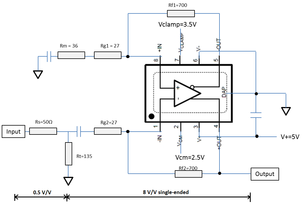
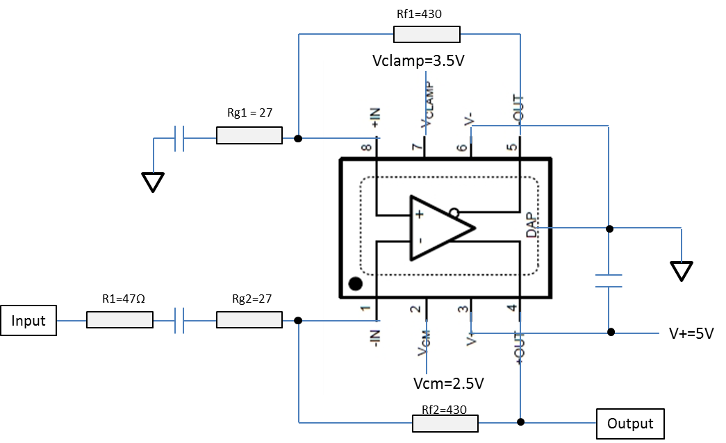
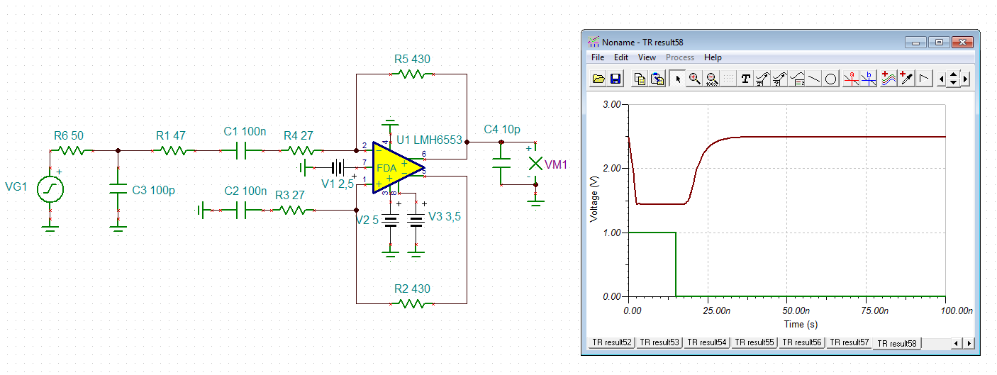
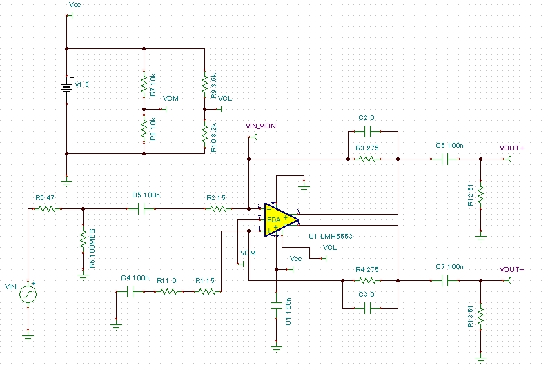
The following is assumed 5V single power supply and single-end input circuit using LMH6553.

1.

Figure 1 of the datasheet shows 59ohm resistor in both path of Vin(+) and Vin(0) like red circle.

While, Figure 58 shows no RT in Vin(-) path.

Which circuit is adequate for single-end input and single power supply circuit?

And should these RT resistors be mandatory components for customer design?

2.

Datasheet shows recommended value of RF in Table 1 and Table 2.

Is it accepted to use different value of RT? (e.g. 400Ω)

If not, what kind of impact is expected with different value?

3.

Customer design is configured in single-end input and 5V single power supply.

What is value of common mode input range?

BestRegards

  • Hi Na na 78,

    the idea of RT is to make the input of this circuit look like an exact 50R load. This is necessary if you want to connect a cable to the input. In high frequency circuits the cabling is usually down by the help of 50R technique. This means, that the driver and the cable must also have an impedance of 50R.

    Kai
  • Hi,

    To answer your questions:
    1. For single ended input and single power supply circuit, I would recommend to use the circuit in Figure 58. In Figure 58, the RT is absorbed into the Rm, where the RM = RT||RS. You may want to take a look at figure 56 as well that defines what each resistor values are.

    When driving the LMH6553 in single-to-diff configuration, it is usually desired to match the source impedance (Rs = 50-ohms in this case) with the active input impedance of the device in-order to minimize any power reflection at high frequencies. The RT is used primarily to provide this matched active input impedance. So, I think it is required to implement the Rt in customer's system.

    2. Yes, there can be a scenario when a different value Rt would be required than what is specified in Table 1 and 2. The value of Rt is primarily determined by three conditions: 1) Device Gain, 2) RF or feedback resistor value and 3) Source impedance (Rs). If you can provide us with these three conditions from the customer, then we should be able to provide an appropriate circuit using the LMH6553.

    3. Do you mean the common mode range of the LMH6553 inputs or the VCM pin that controls the output CM voltage? On a single +5V supply, the input CM voltage at the LMH6554 inputs IN+/- can typically be 2.5V+/-1.2V or +3.7V/1.3V. Similarly, the VCM pin voltage that controls the output CM voltage can typically be from 2.5V+/-0.81V or +3.31V/+1.69V.

    Best Regards,
    Rohit
  • Hi Kai

    Thank you for your reply.
    We will consider 50ohm termination.

    BestRegards
  • Hi Rohit

    Thank you for your reply.

    I understood 1, 3.

    Regarding to question 2, I add infomation about a circuit the customer is configuring now.

    As shown in this figure, it offers single-end input to single-end output configuration, with 5V single supply.

    Gain  ( single end) : 7.96

    Feedback resistor : Rf = 430ohm

    Source impedance : Rs = 50ohm

    Vclamp=3.5V

    Vcm=2.5V

    Could you please check this configuration and please suggest modification if any?

    BestRegards

  • Hi Na na,

    there are some mistakes in your last scheme. Please have a look at your first scheme again. The - input of LMH6553 sits virtually at signal ground. So, the upper 59R resistor and the upper 255R resistor are in parallel, forming an input impedance of about 50R.

    In order to keep the wiring of LMH6553 symmetric, the feedback loop arround the + input of LMH6553 imitates the impedances seen by the - input. So, the 49.9R resistance in series with the 100n cap imitates the hidden source impedance of the driver, which sits in parallel to the upper 59R resistance.

    Or by other words, the + input and the - input of LMH6553 must see the same impedances to signal ground. In the first schematic this is fullfilled. In your last schematic this is not fullfilled.

    Kai
  • Hi Kai

    Thank you for your reply.

    I modified following circuit based on Figure 56.

    I believe this will offer Av=16 (8V/V with single-end out) and it will match for 50ohm system.

    Could you please review it?

    BestRegards

  • Hi Na na,

    I don't think that such a high gain is possible with this chip in a 50R system, because when chosing Rg=50R and omitting Rt, Rf must be much higher than the maximum recommended value (325R).

    Let's see what Rohit means...

    Kai
  • Hi,

    I think the circuit you have posted should work with termination resistor Rt = 135-ohms, and Rf = 700-ohms providing an input impedance match of 50-ohms.

    However, one thing I wanted to point out is that due to the input impedance matching, you will lose 0.5V/V at the input. As a result, the total single-ended gain from input to single-ended output will be 4V/V. If the input frequency is not very high and the input interface trace is not very long, then you should be able to reduce the Rs to 10 or 20-ohms, and subsequently change Rm = Rs||Rt. This change will achieve higher gain from input to single-ended output and keep both paths symmetrical. For example, with an Rs = 20-ohms, the Rm will need to be 17.5-ohms.

    Also, if the input and output are single-ended, then is there a reason to choose a fully differential amplifier such as the LMH6553? I think an op-amp can be used here instead and would be a cleaner solution. Is it primarily because of the LMH6553 clamping feature that the device is being considered here?

    Best Regards,

    Rohit

  • Hi Rohit

    Thank you for your reply.

    We can consider to change Rs.

    > Is it primarily because of the LMH6553 clamping feature that the device is being considered here?
    Yes. It is intended to control output swing level using clamping function even if the input is large.

    So if 1Vpp and 50MHz input pulse is supposed, we expect the single-end output could be limited 1Vpp with Vcm=2.5V and Vclamp = 3.5V.


    BestRegards

  • Hi

    Please tell me your view about following situation.

    Based on the following circuit, we saw an output that had slow changing at falling edge against input pulse.

    Input: Upper figure, Output : Lower figure

    I could not get why it has slow change only at the falling edge.  

    As you expressed, is it cause of input termination? Or any other cause?

    What kind of cause do you think? Please tell us anything thinkable.

    BestRegards

  • Hi Na na,

    was it measured with your original and faulty circuit from 26 march?

    Kai
  • Hi kai

    It was measured with the circuit which is not along with Figure 1 or Figure 58. (It is the last figure I attached.)
    The circuit has not modified yet to meet recommendation.

    BestRegards
  • Hi Na na,

    TINA-TI simulation shows that a capacitance at the input can be responsible for that behaviour:

    Cable capacitance could do this. This shows how important proper cable termination is in high frequency applications.

    Kai

  • Hi,

    I would recommend you to modify the circuit for input termination as provided in my previous post. As Kai mentioned, not having proper input termination at high frequencies could result in long settling due to input reflections caused by the cable.

    Best Regards,

    Rohit

  • Hi

    Thank you for your cooperation.

    I have to apologize that I offered wrong information.

    Let me indicate the measured point using following circuit.

    The measured wave forms were obtained at the point ① and ②.

    A wave measured at point ① :

    A wave measured at point ② :

    The wave at the point 1 seems to be not so dull.

    Input to the LMH6553 is a pulse from I/V amplifier output.

    And a cable is not used at AC coupled input. (10mm wired on the single board)

    BestRegards

  • Hi Na na,

    do you see the long settling at measuring point 2 with the scope being connected to measuring point 1 at the same time? Or by other words, are both scope probes simultaneously connected to the circuit?

    Kai
  • Hi Kai

    It was not measured at the same time, it was obtained individually.

    BestRegards
  • Hi

    Let me consider recommended feedback resistor.

    I changed Rf from 430ohm to 275ohm with the gain around Av=16 ( Av=8 in single-end out). 

    Please refer following simulation result.

    1. Rf=430, Rg=27 

    2. Rf=275, Rg=15

    Smaller Rf is, dulling at the output seems to be mitigated.

    In addition, I can see the recommended feedback register is 275 or 325 by the package, in the datasheet page 19.

    Questions 1

    Is there possibility to make output dull if larger Rf is selected?

    Question 2

    Can you offer recommended Rf and Rg to set gain as 16?

    Questino3

    Is there maximum gain for LMH6553?

    BestRegards

  • Hi Na na,

    yes, current feedback OPAmp can only work properly with feedback resistors lying in a limited range. So, increasing Rf above the recommended value can result in improper performance like increased settling time.

    Kai
  • Hi Kai

    I apologize for this late reply.

    What do you think of limitation of gain settings?

    I wonder if it is feasible to set 16V/V gain ..?

    BestRegards
  • Hi Na na,

    the gain limitation in datasheet to 12dB (table 1) has mainly to do with the termination needs when connecting a 50R cable to the input. So, without having a 50R cable to connect to the input you could try to increase the gain like shown in figure 62.

    But keep in mind, that the LMH6553 will come to its limits when increasing the gain so much. I think it would be better to use two cascaded OPAmps and split the gain onto two gain stages.

    Kai
  • Hi Na,

    Is there a reason for the LMH6553 to be such a high gain of 16V/V when the input at measurement point 1 is already at 1Vpp? If the input is at 1Vpp at measurement point 1, then the actual output will come out to be 16Vpp which is significantly high clamp overdrive (~ 1600%). The clamp overdrive specification in the datasheet is only for a 100% overdrive.

    I certainly think that the output long settling (measurement point 2) during the input falling edge is the recovery time from the significantly high clamp overdrive. Would it be possible to replicate the setup with lower gain setting (say 2V/V) and see if the output long settling issue is resolved?

    Best Regards,
    Rohit