This thread has been locked.

If you have a related question, please click the "Ask a related question" button in the top right corner. The newly created question will be automatically linked to this question.

INA168: Glitch on output when VIN between 0.7V and 1.2V

Part Number: INA168
Other Parts Discussed in Thread: INA180

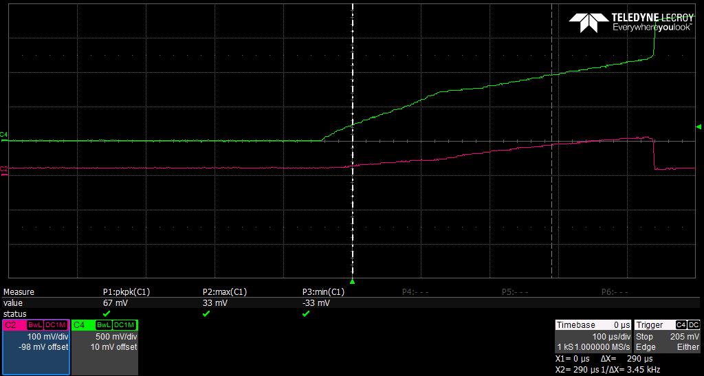
I have noticed that I get a glitch on the output of the INA168 when VIN+ is between 0.7V and 1.2V.  This is a potential issue for me as my system has a slowly ramping input voltage and it's possible that the output glitch can be seen by my micro before the micro VDD is established.  I get the same glitch as the system voltage ramps down - when it reaches 1.2V the INA168 output spikes up to 300mV, which then ramps down with the input voltage.

Is this normal, expected behavior?  There is no current passing through the sense resistor at these times so I would expect the output to be zero.  

If this IS expected behavior, is 300mV the expected size of the glitch?  Or could it potentially be higher?  300mV is right around the max I would want to apply to the GPIO of an unpowered microcontroller, if another INA168 could have a different glitch (say, 700mV) then this could be a much larger problem.

  • Hi David,

    you wrote that you connect the output of INA168 to the GPIO of a microcontroller. Is this a ADC-input or is it a digital input? If you only feed a digital input you could insert a transistor switching stage. This would fully isolate the output of INA168 from the µC's digital input.

    Another method to suppress the glitch, at least partially, is to use an output filter like shown in figure 12 of datasheet.

    Have you scope plot of output glitch?

    Kai
  • Hello David,

    Thanks for considering to use TI in your design.  I presume the glitch occurs when the INA168 is powered on.  If not, it is possible although we do not have data to confirm. Alternatively, if the device is powered on, the glitch you are seeing is something we would expect to see for a quick change in the common mode voltage.  Typically we have a plot of such behavior in our datasheets like the one I have below (taken from the INA180 datasheet).  Unfortunately, this is an older part and providing this corresponding specification was not a standard TI practice at that time.  However, from the second figure below (taken from the INA168 datasheet), I would expect the glitch to be more negligible if it the rising/falling slope can be constructed from harmonics lower than 5kHz. As for the normal size of the glitch for a high slew rate changing common mode I would need to take multiple measurements to determine this.  In which case I would like to know exactly your operating conditions, including the startup and and transition duration.

  • Hi Kai, Patrick,

    The INA168 output is going to the analog comparator pin on my micro.  I take advantage of the adjustable threshold in my firmware so using an external transistor would not be an option.  Coincidentally I am using an output filter like figure 12, although with the goal of smoothing the output, rather than suppressing this glitch.

    Patrick - perhaps 'glitch' is not the right term, as it's not related to a transient or a change in the input.  The issue is that the output is driven to ~300mV when the input voltage is between 700mV and 1.2V.  I realize that this is below the normal operating voltage of the part, but it still can cause problems if the VDD for the microcontroller is not present yet.  I've attached two pictures of oscilloscope traces, showing the output (yellow) as the input voltage (blue) slowly increases, and as it decreases.

    The above were taken as I slowly increased the voltage from a power supply.  Here is the output when I simply plug in the system - VDD (blue), which is the output of an LDO, rises quickly, but the INA168 output is, for about 1-2mS, higher than VDD.  It's still at a pretty low voltage, but the fact that this happens at all is a cause for concern.

    I saw similar results from two parts that I tested.  My fear, though, is that some other parts might output a higher voltage than 300mV (which could be too high for an unpowered micro) or another LDO could ramp up slower, allowing the INA168 output to reach a higher voltage, or for longer, while VDD remains low.

    Let me know any thoughts on this.

  • Hi David,

    you could clamp the glitch at output of INA168 by the help of a PJFET like the PMBFJ177. This FET shows a 100R short circuit between source and drain when the gate source voltage is 0V and it becomes high ohmic when the gate voltage is some volts more positive than the source. You can connect the gate to the supply voltage of microcontroller.

    If the clamping across the load resistance is not sufficient you can form a voltage divider with the PJFET as clamp.

    Kai
  • Hello David,

    As we do not have that operating condition performance characterized right now, I would need to do several measurements of several samples from different lots to give you a definitive answer, which potentially can take longer than you are willing to wait.  

    However for now, I would recommend a common-mode filter on the input and a RC filter on the output like in the figure below. These should help your condition, unless you plan to be measuring current on high frequency signal lines.

  • Hi Patrick,

    This is actually for an existing design - my primary goal is to determine whether this behavior is causing any problems in the current system.  I think that what I have observed should not harm my microcontroller - the 300mV 'glitch' should be OK even when the micro is unpowered, and the faster-rising output only gets about 100mV above VDD, which should also be OK.  

    Regarding sampling parts from different lots - my fear is that the 300mV glitch could be higher in different lots - even a little higher than 300mV would start to be concerning and anything above 600mV could definitely harm or destroy the micro.  So, I would be interested to know the results of sampling from different lots, if possible.

    Or, if the maximum glitch voltage is something that could be determined from the design itself, that would be sufficient and I'd be interested to know what that voltage might be!

  • Hey David,
    So I took measurements on three different samples. I also did a test on one sample with different output resistor values. While taking these measurements, I noticed that the output actually rises with the common mode up to ~1.2V and then subsequently drops back to ground (assuming there is no differential across the shunt). I also noticed that these output values are static for any given common mode voltage in this range. The max values I measured for each sample are as follows:

    Test 1: Output with 1K output resistor
    S1: 115mV
    S2: 112mV
    S3: 116mV
    Test 2: S3 output with different output Resistance value
    500: 70mV
    1k: 116mV
    10k: 558mV

    The supply voltage for these measurements was 5V. However, I got roughly the same values when the supply was 3.3mV. All measurements were from the same lot and I cannot get any different lots anytime soon. Also, after speaking with my team and management on this issue, the consensus is that this operating condition is outside of our specifications and we will not modify the datasheet based on whatever I find. That being said, my tests were relatively consistent with little variation. If you give me the value of your output resistor, I can confirm if my device performance for your conditions is the same (I suspect my devices come from a different lot).
    So if you would still like to proceed with this device, but with a some safeguards for your microcontroller, the simplest, cheapest approach would be to use RC filters on the input and output that give your microcontroller sufficient time to turn on. However, if you can afford the board space and cost, you may try using a transistor to short the output to ground until your microcontroller is ready.
  • Thanks Patrick. Can you clarify a few things for me?

    When you said the output "rises with the common mode up to 1.2V" - do you mean something similar to the first picture I posted in this thread, of the output voltage increasing as I slowly increased the common mode voltage? Or something else?

    I'm also confused by this and the next statement, that the output values were static for any common mode voltage in the range. Did the output rise with the common mode voltage, or did it remain the same?

    If the output fell down to GND after the common mode voltage rises above 1.2V, what was the potential difference between a supply of 5V and 3.3V?

    Did you do this test by slowly increasing the system input voltage? Or by simply turning on the input voltage (to either 5V or 3.3V) and watching the output voltage ramp up?

    Do you have any oscilloscope shots of your testing? Perhaps that will help.

    My system is currently using a 10K output resistor, so the fact that I measured 300mV while you saw 558mV is very concerning to me. Please let me know the answers to the above - the exact situation(s) where the output might rise to 558mV is very important information, as it will determine whether the INA168 output could be dangerous or not.
  • Hey David,

    Sorry for the confusion.  Below are some scope shots of some of my measurements.  These all correspond to the 1 kΩ load resistor with Vin+ and Vin- shorted. For each measurement, I did not adjust the common-mode until the supply was at 3.3V or 5V.  The pink trace corresponds to the INA168 output, while the green trace corresponds to the VCM.

    In the first figure I applied a rising common-mode voltage with a rise ratio of 1mV/μs.  Thereupon in figure 2 I applied a falling common-mode voltage.  Then in figure 3, I slowly dialed up to the common-mode voltage that produced the largest output in this sub-recommended range (~1.2V) and left the voltage there, (this was what I meant by static).  Below these figures, is the schematic for the test used in figure 3, that yielded the 558mV you are concerned about.

  • Hi David,

    it should be added, that it is absolutely normal that the output of such an analog chip can emit an unpredictable potential during power-up and power-down. It's the standard behaviour of all OPAmps. There's always a certain threshold the supply voltage must exceed to make the chip work properly. No chip is correctly working down to a supply voltage of 0V.

    If the succeeding circuit cannot withstand these power-up and power-down glitches one remedy is to clamp the potential to a sane level during this moment. So, I repeat my hint to use a p-channel JFET like the J177 to clamp the output voltage of INA168.

    Kai
  • Hi Patrick,

    Thanks!  That definitely makes things clearer.

    So, there is one significant difference between my circuit and yours - I have pins 3 and 5 tied together, so that rising VCM is also the power source for the INA168.  And as a smaller difference, my output resistor is 10K.

    Do you think you can repeat the tests, but with a 10K output resistor, and connecting VCC to VIN+?  I wonder if that is why I am seeing a different voltage than you are (300mV vs 558mV).

    The datasheet makes it sound like VCC is completely independent of VCM - could I power VCC from the output of my LDO (3.3V), even those VCM is as high as 30V?  Or even better, from a microcontroller IO pin?  Can you test what the output does when VCM is rising but VCC is 0V?

  • Hello David,

    I finally ran those tests. If VCC and VIN+ are tied together, I get a max output of 312mV at 1.17V VCC.

    Your interpretation of the datasheet is correct, the VCM specification is independent of the VCC. So you can power VCC from a source much smaller than VCM. However, your output max will not exceed VCC. Having device supply grounded while VCM is some voltage under 75V should not destroy the part. However, for linear operation, the VCC should at least have the minimum recommended operating voltage of 2.7V.

    For VCC = GND while VCM is rising. The output was 0V in my test.
  • Thanks Patrick.  For your test with VCC and VIN+ tied together, was your output resistor 10K?

    If so, it sounds like your results are matching mine, so with any luck different batches of the part will have a similar maximum output voltage of ~300mV while VCM and VCC are rising are around 1.2V.

    Also good to know that the output will be limited to VCC, independent of VCM.  That may be the right fix for the future, to power the device from either the same rail as the micro, or from an IO on the micro itself.

  • Hey David,

    My output resistor was 10k.

    Glad to know we could assist you. Let us know if you have any additional questions or concerns.