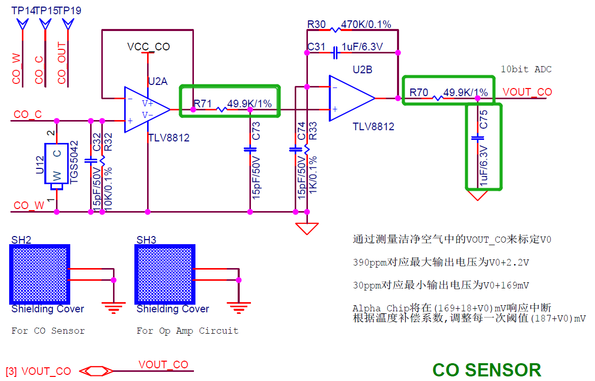
Hi Team,
I'm using TLV8812. Please kindly help to review the schematic as blow, any comment will be appreciated. Thanks very much.
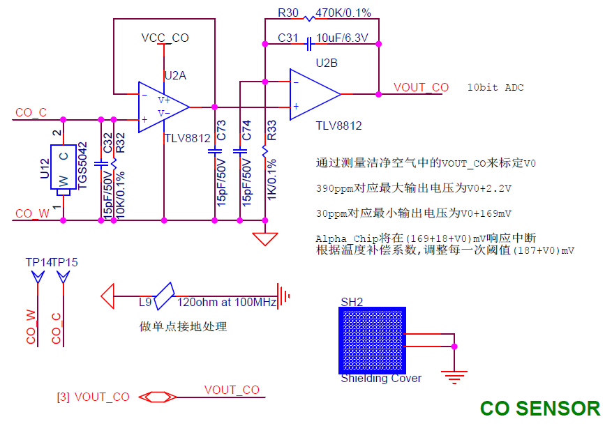

Hi Team,
I'm using TLV8812. Please kindly help to review the schematic as blow, any comment will be appreciated. Thanks very much.