This thread has been locked.

If you have a related question, please click the "Ask a related question" button in the top right corner. The newly created question will be automatically linked to this question.

OPA2333: Conversion accuracy

Part Number: OPA2333
Other Parts Discussed in Thread: LM7705, OPA333

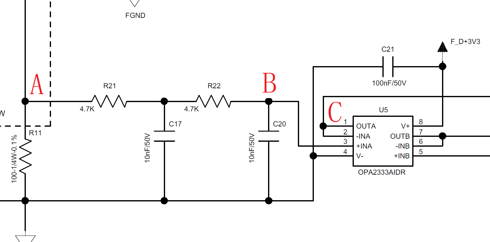
The circuit schematic is shown below.Using OPA2333 as a voltage follower.  The conversion error is large, why?

FLUKE(754) test circuit at 30 ° C.  UA=1V. UB = 0.9983V.  UC = 0.9997V. 

IB of OPA2333 is 200pA,IOS of OPA2333 is 400pA. Why UA-UB=1.7mV? Why UC is greater than UB?

  • Hi Rengui,

    have you taken the finite input impedance of your "Fluke 754" into account? It will form a voltage divider in combination with R21/R22.

    Kai
  • Hi Rengui,

    Issues like this are usually related to some unexpected, secondary effect such as leakage current. A common issue encountered when parameters like voltage offset, or input bias current don't appear to be correct is a lack of PC board cleanliness. Residual solder flux can set up leakage current paths on the board and the current flows between various nodes. These leakage currents corrupt the dc performance of the circuit.

    When we assemble test boards and EVMs for our precision op amps such as the OPA2333AIDR we use solder having water soluble flux. Once the soldering has been completed the board is cleaned using DI water in an ultrasonic cleaner. In actuality the boards are usually subjected to two separate cleaning cycles with fresh DI water. We find that second cleaning can make a difference in dc performance obtained compared to a single cleaning.

    If it isn't a cleanliness issue, check the output of the OPA2333AIDR with a 10x probe and DSO. Make sure the output is relatively noise free and there are no signs of oscillation. If there is noise pick-up or oscillation present that will affect the dc measurements. Make this check with the Fluke 754 DMM connected into the circuit. The leads may be picking up noise and injecting it into the circuit. The DSO would make that evident if it is an issue.

    Regards, Thomas
    Precision Amplifiers Applications Engineering
  • You're right.

    I neglected the influence of FLUKE's input impedance on the circuit.
  • OPA2333 output signal for ADC acquisition, need to connect a small load to the ground? why?

    Some colleagues around me said that the circuit is more stable.

  • The schematic diagrams of CH2_A, CH3_A, CH4_A. The four signals are the AD7124 inputs.
    Between the OPA2333 and the AD7124 is a low pass filter (10kΩ and 100nF). When collecting, the channel has crosstalk. When 100nF is removed, crosstalk disappears. The code value of CH1_A before the capacitor is removed is 1V, and the code value of CH2_A is 20mV. After removing the capacitor, the code value of CH1_A is 1V, and the code value of CH2_A is 0mV.
  • Hi Rengui,

    this is no crosstalk. The output of OPA2333 cannot fully go down to 0V. Have a look at section 6.6 of datasheet ("voltage output swing from rail"). It's the remove of 100n cap which makes the output signal become incorrect. Do not remove the 100n caps at inputs of ADC.

    Kai
  • There's another issue with the protection diodes: These are Schottky diodes with big leakage currents. These can additionally introduce errors when they flow across the 4k7 resistors and produce a voltage drop.

    Better use a BAV99 or even BAV199 and connect it between R16 and R70.

    Kai
  • Hi Rengui,

    If the Schottky diodes had been included in the first schematic the discussion would have involved the potential for diode leakage current that Kai mentioned.

    The OPA2333 has internal, low-leakage input ESD protection diodes. These diodes can safely handle up to 10 mA continuously should one become forward biased. External diodes can be added to handle even higher current, but such diodes - especially Schottky diodes, can introduce high leakage currents. Conventional small-signal silicon diodes such as the 1N4148 often exhibit much lower leakage current than a small-signal Schottky diode.

    Additionally, the resistors in the input low-pass filter add nearly 10 k of resistance in series with the non-inverting input. This resistance limits the maximum current that can flow into the OPA2333 input should an electrical overstress (EOS) event occur. Datasheet Section 7.3.2, Input Voltage, describes the input current protection provided by the added series input resistance. Thus, the circuit may be sufficiently protected without adding the external diodes.

    The OPA2223 is a unity-gain stable operational amplifier. Adding a capacitive load to an op amp reduces the phase margin and may result in instability, or poor transient response, in some cases. The circuit shown above has a 10 k resistor (R21) in series with the OPA2333 output and where it connects to C34 (100 pF?). That resistor will isolate the OPA2333 output from the capacitance and there should be little, if any degradation of the phase margin.

    Adding the 10 k resistor from the OPA2333 output to ground will increase the output current sourced to the load, compared to when the resistor isn't present. The increased output current lowers the op amp's open-loop output impedance (Zo). That can improve the phase margin and enhance stability. The load resistor shouldn't be needed in your OPA2333 circuit.

    Regards, Thomas
    Precision Amplifiers Applications Engineering
  • Hi Thomas,
    Thank you for your reply.

    When 0mA is input, R71 is 10k, and the AD7124 code value is about 160 (6mV). R71 is modified to 100Ω, and the AD7124 code value is 0 (0mV).

    TI employees Xu, Iven suggested that R71 should be within 100Ω, otherwise the output load will cause the op amp to work unstable. I accept this statement.

    In order to maintain the channel circuit filtering frequency, R16 and R70 are changed from 4.7k to 10k, C6 and C7 are changed from 10nF to 100nF, and when inputting 0mA, the AD7124 code value is about 160 (6mV),D30 is deleted, and the code value is 0.Why does the diode affect the loop, don't understand?
  • The problem I have described, please help me.

  • Hi Rengui,

    I already told you, that the OPA2333 cannot fully go down to 0V at its output. No OPAmp powered by a single supply can do this. There's always a dead zone of some tens of milivolt. But you could add a small negative supply voltage by the help of LM7705, or similar. Another method is to introduce a DC offset and to use the differential inputs of ADC.

    Kai

  • Hi Rengui,

    Iven Xu has spent time here at our location and understands operational amplifier stability well. If he has determined that R71 can be reduced to 100 Ω for the particular capacitive load you have specified, then that should be a good, valid assessment and conclusion.

    It is difficult to know without conducting a thorough investigation why removing D30 results in the output going to zero. There is a possibility that a small dc voltage is being developed as the result of the D30 rectifying the non-inverting input bias current. The OPA2333 is a chopper operational amplifier. There is switching occurring at the inputs of the OPA2333. The input bias current is mostly very low and constant, but when the switching takes place there are current spikes generated as the result of charges being transferred within the input switch structures. These spikes are very short in duration but much higher in level than the nominal, non-switching input current levels. My thought is D30 is rectifying the pulses and the filter capacitor smooths the pulsating dc ripples. That small voltage is being interpreted as a voltage-offset component.

    You will note that the OPA2333 inverting input does not have the back-to-back input diodes and there doesn't seem to be any unexpected current or voltage at that input.

    I would remove D30 from the circuit as I suggested previously. You now have 20 k of input series resistance adding even more input current protection.

    Regards, Thomas
    Precision Amplifiers Applications Engineering
  • Hi Thomas:
    I submitted a question about OPA2333 again, help answer it, thank you!
  • Hi Thomas,

    How is the conversion error of the OPA2333 in the circuit evaluated?

    I know that the bias current and the bias voltage introduce an error. The bias voltage error in this circuit is 10μV and the bias current error is 1.68μV(200pA*9.8kΩ).

    Looking at a piece of data before seeing noise and open-loop gain will introduce errors. How is this error evaluated?

  • Hello Rengui,

    I have not seen the term conversion error applied to operational amplifiers, but what I think you are asking about is the total error observed at the OPA333 output due to voltage offset and input bias currents.

    Rather than get into a lengthy explanation here about how each component I will refer you to the TI Precision Labs series:

    Section 2. TI Precision Labs - Op Amps: Input Offset Voltage and Input Bias Current

    You can access the session here:

    The two sections require about a half-hour. You should have a good idea how to proceed in determining the total error after viewing them.

    Regards, Thomas

    Precision Amplifiers Applications Engineering 

  • Rengui,

    We haven't heard back from you so we assume this answered your questions. If you need more help just post another reply below.

    Thanks
    Dennis