This thread has been locked.

If you have a related question, please click the "Ask a related question" button in the top right corner. The newly created question will be automatically linked to this question.

INA240: A2 REF1+2 RVRR 2uv/v

Guru 54077 points
Part Number: INA240
Other Parts Discussed in Thread: INA282, TIDA-00909

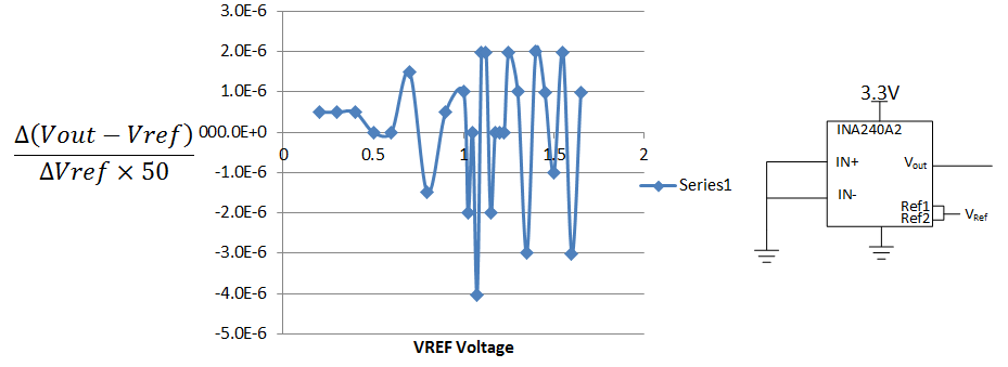
It would seem the datasheet analysis section leaves out very important factual info, REF1+2 divides A2 RVRR (2uv/v) effecting amp gain and noise immunity. Effectively lowers disclosed REF noise rejection and increases 50v/v gain to near 100v/v.

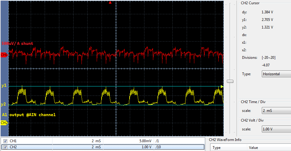
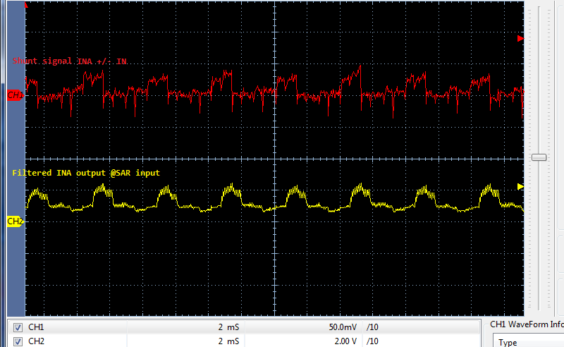
A 500uv/A shunt should produce 25mv/A in all disclosed REF configurations and actually produces 75 - 100mv/A when REF's are tied together. Tina INA240A2 DC or transient analysis macro is not producing correct output results for REF1+2 tied to external reference. Otherwise certain configurations of REF pins mislead customers in the design stage by plotting false data. Tina INA240 model is not disclosed as being DC model only and should produce correct transient analysis plot results for different configurations of REF pins and chosen shunt resistance values.

When REF1+2 pins are tied to an external reference the A2 50v/v gain nearly doubles, e.g. 50% error occurs as REF1+2 are below mid supply (+1.65v). Ideally we need to reduce REF1+2 below our +1.225v external precision reference to reduce output gain error %, not increase error as stated in datasheet, e.g. REF1/2 pins are above ground. 

That part of the datasheet as from our evaluation (REF1+2 external reference) violates Tina models and the electrical specifications section of disclosed amplifier gains. Perhaps lab can revisit the electrical specifications/analysis and total error sections to list WA for errata being disclosed?

  • Past live experience with 282 and 240 for REF1 / REF2 output set mid supply, a resistor network was required to divide output signal. Seemingly current measurement would be less prone to create random output transients when only reducing threshold voltages REF1+2 versus resistively diving the output REF1/2 mid supply 3 or 4 times.

    However when REF1+2 are common, above +1v but below mid supply (1.65v) the non-inverting input incorrectly multiplies the signal across the shunt by some undocumented gain factor. We have past reduced output magnitude and more closely followed shunt CMM REF1/2 set mid supply producing unknown error % in the R divided magnitudes. Attempts to improve the precision by adding external reference REF1+2 set below mid supply produced the effects mentioned in first paragraph. Perhaps as REF1+2 are made just above GND potential (450-500mv) the output precision would improve from <1v external reference. If that were not true then REF1+2 tied to ground would produce large output error % being far below midsupply.
  • Hello BP101,

    We are looking into issue.  I am going to run some tests in the lab to see if I can duplicate some of the results you are getting, this may take a day or so though.  In the mean time though, we do discuss how the gain works in this thread.  Additionally, there is a method to calculate the gain error that occurs when an external voltage divider is connected to both Ref Pins posted below.  From the details you provided before, the gain error should be 2.08% for your LDO operating at 1.225V sinking 100uA.  However, I will run tests with a 12.5KHz PWM Vsense signal and see if I can verify your claim.  Have you considered placing a buffer between the voltage divider and the Ref pins?  Also, what kind of ADC are you using (Summing approximation or a delta sigma)?  Are you placing a fully differential amplifier on your Ref pins and out pin?

  • Patrick Simmons said:
    for your LDO operating at 1.225V sinking 100uA

    That is 1.225v precision reference LM4041 powers three INA240's REF pins. Note when we parallel 50k (REF1+2) makes 25k further reducing 2uv/v RVRR to some undocumented value as three INA share reference voltage source. We ? how R2=125k behaves in the divided network of three INA sharing the same reference. That is the only other thing being different from earlier tested, each 240 set mid supply (REF1=VS, REF2=GND). 

    We isolated the 3 INA REF's yesterday each one share +1.225v via separate branches (R5=9.1k, R6=6.8k) set each output near 580mv.  That of course lowered comparator trip point by roughly 300mv, not great. However transient response pulse gain remained nearly the same and 15n output filter now over compensates. So far dividing mid supply output gain via divider seems to produce better results to control excessive transient pulse +/- amplitudes. Sadly Tina plots of that output divided configuration are no aid to also verify the results via calculator makes it difficult to believe the plots.

    The INA240 is not behaving well at faster PWM duty cycles thus only produces faster output transients. We removed Johanson X2Y 1n filters on +/-IN made no difference transients being any less. It would seem that sharing of a single reference LM4041 even with R5/R6 isolation impacts the gain of all three INA in a bad way. It seems INA experiences cross talk between the REFs via the source voltage LM4041 thus exponentially increases gain relative to any single INA output gain. Seemingly that explains the gain of (75-100mv/A) on any single INA output. Tina plots of single INA produces 21.8mv/A with R5/6R divides +1.23v precision reference.

  • Patrick,

    Your diagram R values differs from one posted at the thread link shown below. What is OR (||) in gain error formula ? perhaps you mean division (/,%) The confusion being how can both R5,R6 predict gain error %? Seemingly gain error should be relative to midpoint voltage input REF1,2 pins in the equation. The top R5=9K1 || R6=6K8 suggests 2.5% error is not believable, more like 50% error occurs according to actual test results. Our +80volt DC power supply internal 100 amp bar (75mohm) digital readout indicates 8 amp peaks, yet INA240's are showing 4 amp peaks in each 80us period.

  • Patrick Simmons said:
    Also, what kind of ADC are you using (Summing approximation or a delta sigma)?  Are you placing a fully differential amplifier on your Ref pins and out pin?

    TI MUC embedded 12bit SAR using 3 channels @2MSPS, one shot timer starts 1.25us blanking window that samples each 80us PWM period. Software determines which phase / INA to sample and concatenates results into digital milliamp values that control PWM duty cycle, closed loop.

    No other amplifiers are being used on output or REF pins.

    A freak thought occurs any single INA current gain may be impacted by ohms law in the presence of another INA. Where the reciprocal divided by the added reciprocals R2 or R3 may be exponentially elevating current gain of all three INA. Tina's minimal transient model ability can not confirm how output current gain might be affected by a copartner INA in the same circuit. For example R2,R3 resistance might be acting more like 41k in that current gain loop.

    Also the REF1+2 voltage deviates between INA's >1mv after installing R5,R6 1% tolerance. That ohms test suggests oddness occurs via a single source REF supply used for three INA with 8R7k series output into SAR channel. Also confirmed via DMM R5,R6 were within 0.1ohms of each other. That slight variation on REF perhaps due to laser trimmed values inside each INA being different among other INA. Yet the 1mv REF difference would add only very slight precision error. So we need full ADC scale 75 amps without burning 2 watt shunts in the process making the A2 seem a good candidate paired with 500uohm shunts. 

  • Hello BP101,

    I managed to run some tests in the lab.  My first test involved looking at an INA240A2's RVRR.  My test setup is illustrated in the diagram below.  At each REF voltage, I measured both the ref voltage as well as the difference between the ref and output.  Then I took the difference between measurements.  Thereupon I divided the change in Vout-Vref by the gain and the change in Vref.  So the ratio of change is plotted in the graph below.

    The values we post in our datasheet are a typical value derived from testing multiple units all exhibiting slightly different performance that fall within a gaussian distribution. So the values I measured are reasonable.  Different devices may exhibit different RVRR and it will also depend on operating conditions.  Lower RVRR is desirable.

    I also did some transient tests with an INA240A2 part.  For mine, I simply have the device setup in a low-side configuration with a function generator providing a 12.5kHz differential voltage to the sense pins with the duty cycle varied between 20% and 80%.  My output appears to be fairly clean and not distorted. It can be seen that there is some noise on my Vref and Vsense signal, this would be due to ground coupling.  As my setup does not have 79V switch nodes, that ground coupling is not as pronounced on my output.  I think you should revisit your layout.  Perhaps a star ground configuration would help.  

    Figure 3 : 20% duty cycle, -24.5mV to 37.5mV Vsense

    Figure 4 : 80% duty cycle, -24.5mV to 37.5mV Vsense

    Figure 5: 20% duty cycle, -9.95mV to 21.95mV Vsense

    I ask about the ADC, because for SAR ADCs TI typically recommends placing a charge bucket filter at the ADC input so there is a large reservoir of charge to pull from when the ADC begins sampling with an initially uncharged internal capacitor.  This is yet something else that might help if you do not already have that in your circuit.

    As for the above R5||R6, that was meant to represent R5 in parallel with R6.

  • Hi Patrick,

    Did some testing on 500uv/A shunt today. Shunt voltage was above 50mv for 4 amps being reported INA. That 4 amps derived via 39n charge filter at ADC input, signal shown capture below.  The 75mohm 100A bar on DC supply, indicates 7.6-8amps measured high side of inverter DC supply. Tina transient model (5mohm shunt) plots CMM is 40mv at 8 amps near what our capture shows. A 500uohm shunt should produce 4mv at 8 amps, not 40mv.  The INA output should be 360mv at 8amps not 2.1v shown in capture.

    The shunts we ordered were 500uohm but act more 5mohm, certainly not producing 500uv/A. Both Digi 2016, Arrow 2018 sold exact same shunt listed as 500uohm, shunt marked (0M50) top. Bet large stack of chips they are 5mohm we received, reason output gain/pulses are so high. Have just ordered another vendors 500uohm shunt at this point as nothing makes any sense. 

    There were more shunt transients above 1v than expected, most being filtered by INA but not all. The PWM rejection seems to be doing some good but not stopping most shunt transients exceeding 100mv. It seems the X2Y was helping to some degree, how much capacitance needs to be determined in silence of Johanson's email questions and the EMI filter diagram shown in their datasheet.

    Scope capture @1000 samples deep rejects higher frequencies (not shown).

  • Patrick Simmons said:
    It can be seen that there is some noise on my Vref and Vsense signal, this would be due to ground coupling.

    An did you notice we have 100n caps on each REF1+2 input. One might deduce that a good thing but in hind sight may act more like charge pump. That is each PWM pulse that comes across VREF input, 100n cap extends RC hold time. Example; even 200p caps near each INA output filter had to be removed, caused false tripping of comparators set threshold. So we also moved cap (39n) near ADC inputs after a series 3R9k where 200p was previously. The INA output is hot into the comparator input with only 4R87K in series, no caps.

    So your RVRR REF/output test is comprised pure DC points with no bypass cap. Also test did not check difference when REF1 being tied to +1.225v reference, REF2 GND. Betting change alone makes RVRR reflect more closely datasheet 2uv/v. Also curious results of your test with 100nf cap REF1+2. The kind of info missing in datasheet as to how best practice placing bypass caps near pins my not be desirable in all cases.  

  • HI Patrick,

    Patrick Simmons said:
    Different devices may exhibit different RVRR and it will also depend on operating conditions.  Lower RVRR is desirable.

    Did you mean to say lower noise levels INA with lower RVRR are more desirable? It would seem higher datasheet RVRR (uv/v) value produces more noise rejection (nV/^2Hz) (input referred) Fig.18, when compared INA282 datasheet RVRR Fig.15 RTI/RTO.

    On second look of 1st test rig shows you tied +/- IN to ground. That seems counter intuitive to any voltage noise (input referred Fig 18) other than simply producing ground noise shown in your top capture. Tina transient analysis shows VS & REF inputs produce much more output ripple for PWM being on +/- IN. That's why it would be good to know if adding bypass caps on REF pins defeats RVRR (NV/^2Hz) or distorts output gain upon any PWM feed back into these two pins.  

  • Hi Patrick,

    Vishay shunts; WLSF2512 (0.5mohm 1%) TRC <20ppm/*C are bit more accurate but even they produce higher CCMV for unknown reasons. The INA output gain becomes increased relative to input bias. Remains unclear why the laws of physics break down in the A2 gain documented 50v/v. Theory tells us we should not have to reduce output gain by dividing it via resistors. Yet that seems the only way the SAR ADC can properly handle the transient trash the INA240 spits out even after placing 15n across each shunt.

    It would seem lower gain A1 might better fit the shunt TRC, even 500uv/A. Yet datasheet suggests to use A3/A4 for higher current 100-200 amps. It would logically seem for 75 amp full scale engineer would choose A2 and very low values shunt microvolt range. There is nothing in datasheet to suggest otherwise A1 would be a better choice for PWM current monitors 0-100 amps. INA datasheet seriously drops ball on side of mayhem in the fits all applications approach they sometimes take. The only real PWM tests TIDA-00909 uses A1 but only in a 16.5 amp full ADC scale, tells us very little the void being left between 16-100 amps!

  • Hello BP101,

    I am little confused as to how you are expecting 360mV at the output when your vsense is 4mV. Are you still using 1.225V for REF1 and REF2? For the test above, I did have a bypass cap for the supply, but no bypass cap for the Ref pins. From the standpoint of saying I want more rejection on my reference voltage pin, I agree that a higher rejection number would be better. However, our specification corresponds to the change in the internal input offset with respect to the change in the Reference voltage. Smaller RVRR means smaller internal offset change. Therefore a smaller RVRR is better.

    As for another debug measure, have you looked at just the INA240 without the ferrite bead, ADC, and comparator connected? I want to isolate these other devices to verify that the INA240 is the sole source of error. With the inductance of your ferrite beads and using one ADC with multiple channels, I suspect there may be some issues with crossover distortion.
  • Hi Patrick,

    After replacing A2 devices with A1 the SAR has better samples but up to 6amps (REF1+2 @1.224v) while dividing software any lower the fault comparator threshold must be set well above mid supply (2.8v). Just as many shunt transients occur INA outputs with 3v3 TVS diodes (1ns response) transients randomly trip comparator fault. There are no added filter caps on +/- IN pins at this time.

    Patrick Simmons said:
    However, our specification corresponds to the change in the internal input offset with respect to the change in the Reference voltage

    Not sure how one believes the words input referred directly mean internal offset. Neither RVRR graph states any such thing. 

    Patrick Simmons said:
    Smaller RVRR means smaller internal offset change. Therefore a smaller RVRR is better.

    However we are seeing a contradiction to that belief as higher RVRR of A1 is producing far less shunt CMM gain compared to A2. Yet A1 still has to high of shunt CMM gain relative to shunt uv/v value. It seems the INA is biasing the shunt since the output voltage is not consistent to +/- IN shunt peak, captured via X1 probe. However we could then via (A1) lower magnitude, software divisor get a much closer sample read via the SAR. A much thinner GUI scope widget trace (amps) is seemingly more evidence counters RVRR claim, less is more. It would appear from these real application test results (A1) the higher 20uV/V RVRR is somehow producing a lower shunt bias than A2 for the very same 500uv/A shunt.

    How can either INA (+/-IN) be changing the shunt bias relative to REF1+2 threshold for the very same shunt R value?

    Patrick Simmons said:
    As for another debug measure, have you looked at just the INA240 without the ferrite bead, ADC, and comparator connected?

    That is not possible in FOC motor commutation, all must report cycle samples to control PWM duty cycles and protect inverter from random faults via comparator reports. Oddly even with the lower A1 20v/v gain the comparator trip point was roughly the same threshold as A2 with REF1+2=1.224v  

  • Below are the scope captures A1 and A2:

    A1: @7.99-8.4 amps 500uv/A shunts, no input filter.

    Notice output peaks reach 2.7v near comparator fault threshold (2.877v) set very high and well over 10mv/A added to REF1+2=1.225v

    A2: 25mv/A output, 500uv/A shunt @7.99-8.4 amps. After below capture added 15n cap across shunt prior to switching to A1 monitors.

    Note REF1+2=580mv yet the output is nearly the same level as the A1 capture above.

  • Even with 1n or 200p caps in the output filter to SAR the gain of both A1/A2 have +1.225v REF1+2 added into the output gain. Notably even with output set mid supply (+1.65v) the A2 output gain had REF (+1.65v) added instead of being subtracted by the INA differential amp. Hence we had to restively divide the INA output to 540mv after being so confused by the bench results over 8 months ago.

    Indeed if TI lab tested the INA240 with 3 INA sharing the same REF via low side monitoring the same results should have been revealed from connecting the INA output into one of TI's SAR ADC's. Tina transient model is not showing these exact same test bench results. So the SAR is likely having some affect on the INA gain to include REF1+2 being incorrectly added back into the INA output gain.

    The REF1, REF2 voltages should only set the floor of the INA output and not be added into the amp gain. The first capture above post should peak @1.3v not @2.7v!

  • Should Ohm's law for multiple parallel branch resistors "Reciprocal of the added Reciprocals" be affecting REF1+2 sharing a single precision reference? Perhaps adding 100k in series each REF should invert the unintended reciprocals. Datasheet suggesting to set output mid supply VS/2 would be inflicted by Ohm's law as multiply INA might exist sharing the same VS power source.

    Note these external and higher R values too would be inflicted by Ohms law fowling INA output gain. On one hand adding 33R3k to each REF would simply cancel out, e.g. no net gain loss! The INA datasheet has not included any notice of REF gain correction formulas, let alone properly disclose strange phenomena being reported in this thread. How has this issue flown under the forum radar for so long, needs to be seriously questioned. Surely TI did not intend on customers circuit to subtract the REF from the INA output gain, wouldn't that be counter intuitive to what a current monitor does?
  • Hello BP101,

    You need to find a way to test isolated individual pieces of your system. There are potentially a lot of sources for error in your system. A few of these include:

    1. Layout – this can exacerbate EMI from high voltage switching and ground bounce
    2. ADC – can exhibit large transient if input source does not have sufficient drive strength or bandwidth. Multi-channel ADC also can experience cross talk.
    3. Excessive filtering – you are trying to measure a 12.5kHz signal at your ADC when the filters on your INA240 output appear to have a bandwidth in the hundreds of Hz, according to your recent post to Guang. This can potentially cause issues with your FOC algorithm.

    I recommend isolating one of your INA240 outputs and measuring to see what it looks like. Then I would recommend having your ADC measure only on one Channel with the other INA240 outputs disconnected from the ADC input pins. After each of those stages are verified to be working as expected or tweaked such that they are working as expected, I would then start integrating more stages of your system in. I know your inverter gates must be driven according to your FOC feedback algorithm. However I am sure there are ways you can impose 120 degree offset trapezoidal waveforms to your gates through a microcontroller or some function generators.

    If you do not attempt to isolate and verify your various system stages on the bench, it will be very difficult to fix your overall problem.

  • Patrick Simmons said:
    3. Excessive filtering – you are trying to measure a 12.5kHz signal at your ADC when the filters on your INA240 output appear to have a bandwidth in the hundreds of Hz, according to your recent post to Guang. This can potentially cause issues with your FOC algorithm

    Necessary to combat +1.225v REF being incorrectly added back into the output gain as the PWM duty cycle increases PWM rejection start to rapidly fail to stop any shunt transients >100mv from inflicting the INA output.  Large filter cap required so the SAR could have proper acquisition plus 880 ohm impedance.

    Guang's explanation does not hold up against scope captures showing SAR acquisition times 80us periods (12.5kHz) are indeed pristine! Also AC rms analysis is required to check SAR input impedance when PWM input signal used in Tina. DC analysis will produce incorrect impedance values. Note users must remove any Ohm meters from model prior to transient analysis or the plots will be infected via 1 volt applied into SAR.

    The problem is not with ADC or SAR, it is directly related to the INA configuration of REF pins and the voltage they are set to. Seemingly being confirmed by TIDA-00909 engineers example REF2 pin grounded sets A1 bias to 820mv and not 1.65v as table 2 suggested. Very likely they too encountered issue with REF which seems to have minor errata relative to how REF pins are being sourced from a precision reference. Why was REF2 tied to ground and did doing so make the differential amp subtract the REF1 input from the 5mohm shunt mV/A? 

  • Patrick Simmons said:
    I would then start integrating more stages of your system in. I know your inverter gates must be driven according to your FOC feedback algorithm. However I am sure there are ways you can impose 120 degree offset trapezoidal waveforms to your gates through a microcontroller or some function generators.

    Patrick A2 was producing fair SAR acquisition REF/2 (1.65v), output being resistively divided down to 540mv via series 1k, 500ohm ground. The 500 ohm after the 1k pulled the gain down and aided REF from adversely inflicting output signal quality. There is undocumented behavior around the REF pins as they relate to the output magnitude without external input filters stopping EMI or PWM transients from inflicting the INA output, seemingly  >100mv. That part of the datasheet text astonishes a belief No input filters are required what so ever but fails to notify at what voltage level input PWM rejection might fail to stop shunt bound transients or otherwise EMI. It would seem the entire PWM rejection subject matter was produced mostly from inline phase monitor point of view.

  • Below capture INA output should appear similar at all PWM duty cycle speeds. This wave form (slower PWM duty cycles) quickly distorts seemingly from the INA input filtering blocking duty cycle changes in shunt current flowing the opposite direction. Perhaps 400Khz bandwidth is not adequate to keep up with the duty cycle changes of PWM generators and the signal becomes somewhat distorted as a result of duty cycle increasing speeds. Obviously the INA datasheet has voids in product disclosure of how to produce a proper balanced current signal at all PWM duty cycle speeds, not just at the slower rate.

  • Otherwise with little to no SAR filter compensation (1n or less) the ADC input more often sees low/high transient peaks. So the INA output has to be well below 1.65v bias and perhaps that helps INA to produce better ADC sample of the shunt current relative to SAR input filters, shown A1/A2 outputs. Perhaps these random peaks (below) are true current but impossible for the SAR to form ratio metric linear sloping from them. The compensated RC filter required for SAR settling inside sample acquisition times relative to lower input impedance mandate excessive roll off to achieve with the INA transient response times. Otherwise they cause random samples of overshoot in the detection of max level current mostly tripping faults on these peaks.  

  • Hello BP101,

    With the addition of the PWM rejection block in the front end, this amplifier does not behave exactly like a totally linear amplifier with a 400kHz bandwidth.  Please refer to https://e2e.ti.com/support/amplifiers/current-shunt-monitors/f/931/t/702644 for a more detailed explanation. Outputs from current sense amplifiers into SAR ADCs should be passively filtered in a way that does not affect stability and with these integrated resistor feedback network amplifiers, the open loop gain is not accessible from the pins.  We use closed loop output impedance to determine resistor and capacitor choices, and http://www.ti.com/lit/an/slya029/slya029.pdf describes this in detail.