This thread has been locked.

If you have a related question, please click the "Ask a related question" button in the top right corner. The newly created question will be automatically linked to this question.

LMH6553: LMH6553 EVAL PCB layout files, SNOA528A, LMH6553SDEVAL

Part Number: LMH6553

Follow up questions relating to this post:

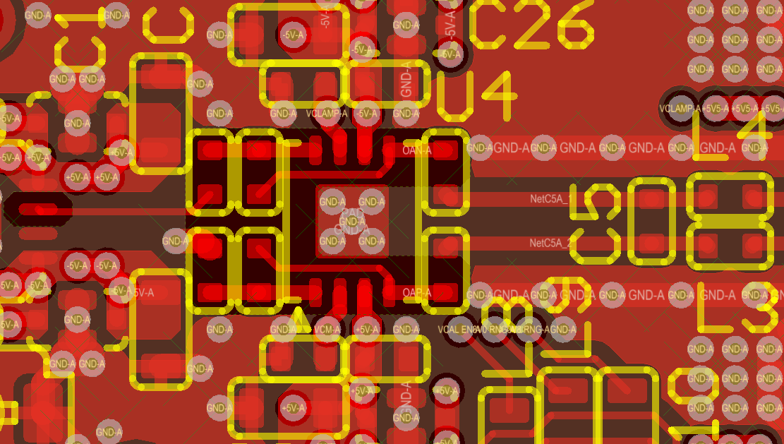
1. What is the layer structure for this board? I would like to know how far the ground plane on layer 3 is below the feedback tracks on layer 2.

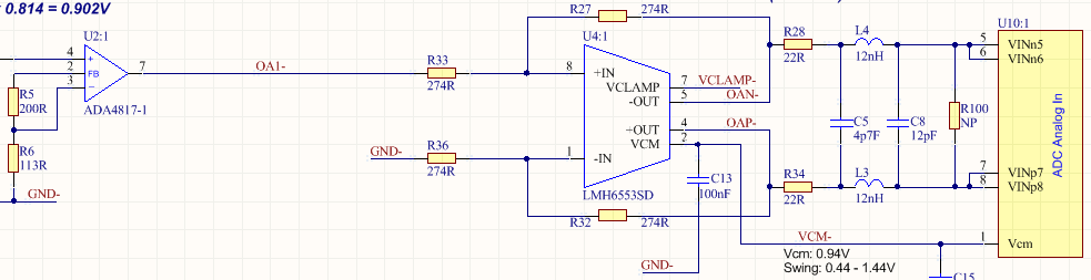
2. In the LMH6553SDEVAL SNOA528A document, Layout Considerations, Item 7. Remove the ground and power planes from under and around the part, especially the input and output
pins.          But on the layout there is ground plane on layer 3 under the input and output pins, so which recommendation should be followed?

3. Why has the ground plane been removed around the VCM and VCLAMP pins? Are these not normally DC levels?

I'm asking these questions because we are seeing some loss of bandwidth on our LMH6553 layout, so any help would be appreciated.

Thanks, Ken

  • Hi,

    We will get back to you shortly. I will see if I can find the original files.

    Regards,
  • Hi Ken,

    Sorry for the delay in reply. To answer your questions:

    1. The LMH6553 evaluation board is 4 layers with 2-oz copper on the top and bottom layer, whereas 1-oz copper on the middle two layers. The dielectric material used is FR-4 High Tg with dielectric constant of 4.8.

    2. The suggestion of removing ground and power planes from under the part, especially the input and output, is applicable primarily for layer 2 which is directly underneath the part. Layer 2 underneath the part is the predominant contributor of board parasitic capacitance. Going one layer further down to layer 3 cuts the board parasitic by square of distance, giving diminishing returns on board parasitic improvement even when the layer 3 ground and power plane is removed.

    3. Because the VCM and Vclamp pins are close to the IN+/- pins, there is a potential of parasitic large signal input coupling from the inputs to the VCM and Vclamp pins. As a result, the ground plane beneath these pins has been removed.

    Would it be possible for you to attach your schematic so that I can take a look? It might be possible to tweak the LMH6553 circuit because of the current feedback architecture, which might enable to compensate for the lost bandwidth.

    Best Regards,

    Rohit

  • Hi Rohit,

    Thanks for these answers to my questions. Some follow up comments:

    1. Do you have the distance from the signals on layer 2 to the ground on layer 3?

    2. Yes, we will implement this approach on our next layout with closed ground on the lower layers to have a more uniform ground plane.

    3. Thanks for the explanation of the VCM and Vclamp pins, but I would have thought that if coupling from the input was an issue then having a ground plane close to them would help. Also, have the decoupling caps close too. I guess I'm not understanding how removing the ground in this case works, could you clarify?

    4. The schematic is as follows. We are seeing 1.7ns rise time before the LMH6553 and 2.7ns after, so it is slowing the signal down.


    And here's the layout. We have 100nF decoupling close to the VCM and Vclamp pins, and 10uF, 1uF & 10nF close to the power pins. The ground plane has been removed on all layers around the input and feedback resistors and the I/O pins. The feedback tracks are on the top layer because we didn't want to use micro-vias (as used in the EVAL layout).


    Any thoughts on how we can improve the bandwidth would be appreciated!

    Thanks, Ken

  • Hi Ken,

    To answer your questions:

    1. I am taking a look at the layer stack up and should provide my reply soon on the distance between signals on layer 2 to ground on layer 3.

    3. The coupling from the input signal IN+/- to the VCM and Vclamp pins is usually not an issue for small signals. However, for large signals it is possible that there is enough ground bounce such that the return current paths will modulate the VCM and Vclamp pins, mainly for single-to-diff conversion where the undriven input is supposed to track the driven input. You are right that having the decoupling caps close to the VCM and Vclamp pins completely eliminates this issue. The other benefit naturally is the reduction of board parasitic cap for the input pins because the VCM and Vclamp pins are adjacent to these pins.

    Some follow up questions/comments in-order to better understand the issue.

    For the rise time issue, are you measuring the 2.7 ns rise time directly at the LMH6553 output or at the ADC? Also, what is the output signal swing or voltage step size at the LMH6553 output ?

    May I know which ADC are you using? The reason I am asking is because the anti-aliasing filter BW could be limited if you have not accounted for the ADC input capacitance. The last leg cap of 12pF needs to be adjusted accordingly so as to not BW limit because of the ADC input capacitance. Also, have you considered removing the anti-aliasing filter completely and seen any improvement in the rise time measurement?

    As such, the LMH6553 schematic looks good and layout seems to be clean.

    Best Regards,

    Rohit

  • Hi Rohit,

    Yes, we are measuring the 2.7ns rise time directly on the LMH6553 output, not after the anti-aliasing filter. The step is 800mV (single ended).

    The opamp output rise time is 1.7ns for a 1.6V step. From the LMH6553 data sheet rise time of 690ps for 2V (I assume differential) I would expect 552ps for 800mV (SE). Cascaded rise time should be sqrt(1.7ns^2 + 552ps^2)=1.78ns, so the LMH6553 output seems about 900ps to slow. So this is where we started looking at the layout for clues.

    I haven't removed the filter but will do some more experimenting.

    The ADC is ISL214S50 and has 13.3pF in.

    Thanks for checking the schematic and layout.

    Just a thought on item 3: I also found the 55600191 evaluation board for the PSOP package and on this layout there are NO decoupling caps for VCM or Vclamp, so that got me thinking that the ground plane has been removed under these signals so that the dynamic response of these inputs could be checked. In any case, we will be keeping the decoupling caps close to these pins on our layout.

    Best regards, Ken