This thread has been locked.

If you have a related question, please click the "Ask a related question" button in the top right corner. The newly created question will be automatically linked to this question.

INA2126: Problem with load cell

Part Number: INA2126
Other Parts Discussed in Thread: REF5030

Hi to all!

I need to capture two signals from two load cell, so i did a circuit with an INA2126 to amplifying this signals and acquiring they with an adc.
This is my circuit

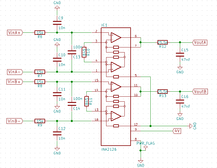
The load cell is supplied using the REF5030 component.

The problem is that this circuit give me the same output regardless if i put a load on the load cell.

In particular, using a multimeter i measure this values for the A side of the ina:

  • V+ = 3.99 [V]
  • Vin+ = 1.46 [V]
  • Vin- = 1.46 [V]
  • Vo = 0.53 [V]

The output of the REF5030 is 2.98[V]. I use a single supply configuration with  V- = Vref = GND.

For the B side of the ina, with no load cell attached, i measure this values:

  • Vin+ = 0.06 [V]
  • Vin- = 0.06 [V]
  • Vo = 3.33 [V]

I have no idea on what is the problem and why i obtain this values in output, so please someone help me to understand why this circuit doesn't work properly?

  • Hi Luca,

    the output of INA2126 cannot fully go down to 0V. The output hangs in saturation and so you don't see a change with and without load on the load cell.

    For the B-side problem you are violating the common mode input voltage range of INA2126.

    The INA2126 is a micropower Instrumentation Amplifier and is not input/output rail-to-rail suitable. Have a look at figure 6 and section 9.1 of datasheet.

    Kai
  • Hi Kai, thanks you so much for the reply!

    I know that the INA2126 isn't input/output rail-to-rail suitable, so i'm not expect this behavior.

    What that i don't understand is why the INA2126 go in saturation.

    From this graph:

    I understand that using this settings, the INA2126 work in the linear zone, or am i wrong?

    This settings are very near to my measure, so why it doesn't work properly, and what i can do to make sure that everything works?

    Also I have did some simulation using TINA software, and using that circuit all work properly in simulation.

    So i get very confused because i not understand where i get in error.

  • Hi Luca,

    the simulator demonstrates that at a common mode input voltage of 1.46V the minimum output voltage for proper performance is 0.8V. So, if your differential input voltage is between 0mV and 8mV the output of INA2126 is in saturation and shows an erroneous output voltage. This is exactly what you observed.

    About the B-side problem: From the simulator you see that your circuit cannot handle a common mode input voltage of 0.06V, because the minimum common mode input voltage is 1V. So, if your input voltage is below 1V the INA2126 will show a wrong output voltage.

    Kai
  • Hi Kai,

    now i understand what happens, i have interpreted erroneous the graph, thanks you for clarifying me this point.

    But now, how I use this component for amplifing the load cell signal? The load cell is balanced, so the difference between S+ and S- is ever near 0 V.

    I have to add some resistor to unbalance the load cell bridge or I change this component with more appropriate component for this job?

  • Hi Luca,

    there are several ways out of the situation. One is to use a small negative supply voltage of -1V (<-0.8V). Another solution is shown in section 9.1 of datasheet, by using a small reference voltage of about 1V. This will cause the output voltage to also have an offset voltage of 1V, of course.

    Unbalancing the load cell by adding a resistor is not a good idea, because this would erode the symmetry of the load cell. This can result in a heavy increase of temperature drift of load cell.

    Kai

  • Hi Kai,
    I'm not an EE, so i need some extra explanations for the your solutions!

    The negative supply voltage of -1V goes into the V- pin? This solution implies only this change in the my circuit above?

    The other solution is simple to me because there is the schema, however i think that i need two REF1004C-1.2 component for the two side of the INA2126 or i'm wrong?
    However, if the output voltage have an offset of 1V, the output range will be between 1.8-4.25 V or i'm wrong?
    In this case the upper bound is great than 3.3V so this is a problem to use the output signal of the INA2126 with an ADC that accept signals from 0 to 3.3V. In this case, I can change the V+ supply voltage to 3.3V?
  • Hi Luca,

    you wrote: "The negative supply voltage of -1V goes into the V- pin? This solution implies only this change in the my circuit above?"

    Yes.

    You wrote: "The other solution is simple to me because there is the schema, however i think that i need two REF1004C-1.2 component for the two side of the INA2126 or i'm wrong?"

    One REF1004C-1.2 would be enough.

    You wrote: "However, if the output voltage have an offset of 1V, the output range will be between 1.8-4.25 V or i'm wrong?"

    The 1.8V will only appear with a differential input voltage of 8mV. With a differential input voltage of 0mV an output voltage of 1V will appear. And 4.25V cannot appear at the output if the supply voltage is only 4V. Ask the TI's calculator...

    You wrote:"In this case the upper bound is great than 3.3V so this is a problem to use the output signal of the INA2126 with an ADC that accept signals from 0 to 3.3V. In this case, I can change the V+ supply voltage to 3.3V?"

    Why not decreasing the gain?

    Kai
  • Hi Kai,

    The TI's calculator show that using the same setting (V+ = 4V, Gain = 100 and Vcm=1.46V) and adding a Vref of 1.2V, the outputs are 0.8V and 3.25V.

    The minimum value is obtained when the input difference is -4mV; and when the input difference is 0V, the output signal is 1.2V. 

    The maximum value is obtained when the input difference is 20.5mV that is 3.25V. 

    So i haven't any of interfacing problems with the adc. 

    Your answers help me a lot! Thanks you so much Kai! ;)