This thread has been locked.

If you have a related question, please click the "Ask a related question" button in the top right corner. The newly created question will be automatically linked to this question.

THS4521: How to improve the output waveform

Part Number: THS4521
Other Parts Discussed in Thread: TIDA-00499, , ADC3441, TINA-TI, INA149, TIDA-00049

Hi,

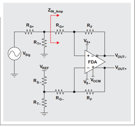
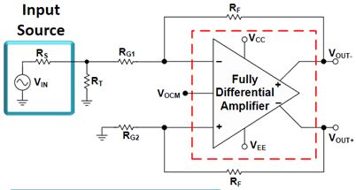
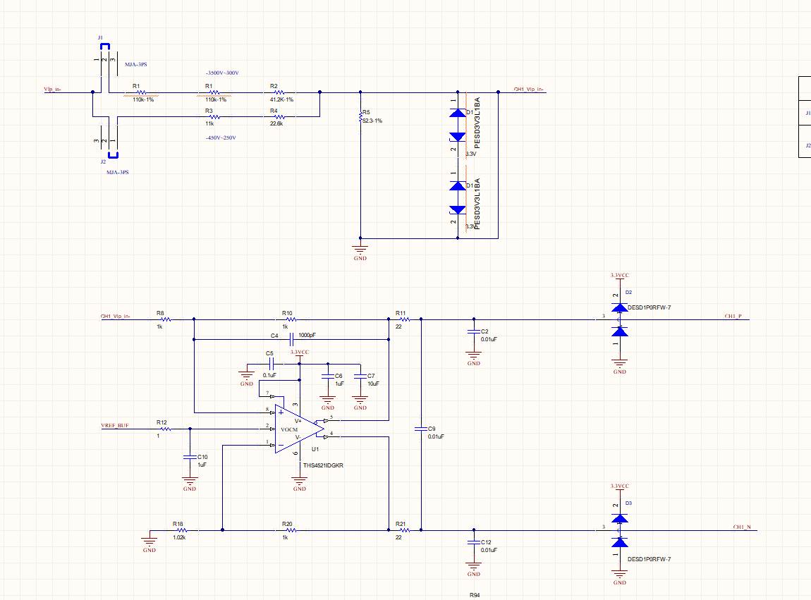
Please help to analysis the attached circuit which is the same with TIDA-00499, but when simulate with TINA, we could find that the output waveform is not smooth, and there is some jitter. In addition, what is the usage of the input Zener diode ?  

Thank you very much.

ths4521_TIna_NO cap NO gnd Vlp_in+ 70V (1).TSC

Best regards

Kailyn

  • Hi Kailyn,

    Thanks for reaching out. I see this post is very similar to this post in which Kai points out the Zener diode is actually an ESD protection diode, and that the jitter is a result of a lack of symmetry in the feedback paths.  There are multiple forum posts about this one topic, can we please consolidate the posts to this forum only? I will comment on the other posts to refer to this thread alone.

    Instead of this thread, this thread, this thread, and this thread, please ask questions here so that we do not repeat ourselves.

    Before answering the questions coming in, please help us understand what you are trying to accomplish. Let me restate my understand of the problem from what has been posted:

    The input: a non-symmetrical, up to 40 MHz signal with a voltage range of -50 to 450 V. However, there may be transients up to 3 kV. 

    The goal: Scale down the input signal to 1.6 Vpp so it can be sampled with the THS4521 driving the ADC3441.

    The problem: You want to use the same circuit as TIDA-00499 but want to change the resistive voltage divider so that it can accomodate 3 kV input transients rather than the 2 kVpp it was designed for.

    Is this correct?

  •  First ,thank Kailyn help me ask this  question.  

    and   To  Micah Brouwer, Yes,your comprehension is very correctly。

    The input: a non-symmetrical, up to 40 MHz signal with a voltage range of -50 to 450 V. However, there may be transients up from  -3500 V to 500V  exactly。

    The goal: Scale down the input signal to 1.6 Vpp so it can be sampled with the THS4521 driving the ADC3441.

    The problem: I want to use the same circuit as TIDA-00499 but want to change the resistive voltage divider so that it can accomodate 3 kV input transients rather than the 2 kVpp it was designed for.  

    but  first ,a very important thing  ,can you  explain  why the  negative input  of the  op  connect to vref  but  not  to GND,What is the purpose of this design??

    then  second ,can you  give me  the analysis  process  of  how  to  get  the  value  of  the resistor  R8 and  R22  ?

    THIRD,in  fact,in design tida-00499, R2,R1and C1 is not populated,it is Equivalent to no RT role ,so  how can it  realize the attenuation?

    fourth,can this design withstand the high common mode voltage of the input  signal?

    finally,Because they are not in the same time zone,It takes a long time to get a reply。I feel that only you currently understand my whole idea.

    So I  still hope that you can continue to answer me and be able to reply to me in the first time. 

    And  i have four questions,so I hope that every question can be answered seriously, don't just reply to one of them.

    o'nly to Micah B Brouwer!I am very  very very very looking forward to your reply.

  • hello,Micah Brouwer, have you see my question ?i am waiting for your answer.
  • You wrote: "I feel that only you currently understand my whole idea."

    Oh, that wasn't nice... :-(

    By the way, it's not nice to start five different threads about the same topic either...

    Kai

  • Hello,

    1) can you explain why the negative input of the op connect to vref but not to GND,What is the purpose of this design??

    This is answered in section 4.2 pg 18 of the design guide, where it states: "The output of the potential divider is applied as the input to the differential amplifier. The input is typically an AC input with a positive or negative transient, which overrides the AC waveform. The AC input must be level shifted by VDD/2. The values are 2.5 V for the SAR ADC and 0.95 V for the ADC34xx family of ADCs."

    So the purpose is to level shift the output so it is centered around 0.95 V for the ADC.

    2) can you give me the analysis process of how to get the value of the resistor R8 and R22?

    We are checking with the author of the TI Design to verify why R8 and R22 were chosen as such.

    3) in  fact,in design tida-00499, R2,R1and C1 is not populated,it is Equivalent to no RT role ,so  how can it  realize the attenuation?

    This is a good question, and we are checking to verify if this is correct. The design utilizes the feedback resistor (R7, 499 ohms) as a part of the resistive voltage divider.

    4) can this design withstand the high common mode voltage of the input  signal?

    Yes, the purpose of the resistive voltage divider is to reduce the input signal to a level that the amplifier and ADC can handle.

    As we did not create this design, please grant us some time to confer with the author to understand why the feedback resistor was chosen as a part of the resistive voltage divider rather than populating R1 or R2. We are working on this and will respond as soon as we have an answer.

    Kai, thanks for you help, this is a rather unconventional circuit. We do not often deal with 3 kV input voltages.

  • ths4521-upload.TSCFirst of all, thank you very much Kai and Micah Brouwer for helping me. the reason why start five different threads ,because The answer of

    some engineer  is really not detailed.so I want to get   answers in this way. please forgive me troubling  you so much.

    1)Micah Brouwer,I know the  AC input must be level shifted by VDD/2,but Have you simulated it?  I have simulated。attached file  is  simulation file 。I  find  when the negative end connected to gnd  and the VOCM connected to VREF,It can achieve the ac input level  shifted by VDD/2,and the  VM6 output is  1.6VPP,Can meet the input requirements of ADC34XX。See the simulation file for details。but when the negative end and the VOCM  all  connected to VREF ,the simulation scope  is  very bad ,it may be i choose wrong R8 and R22.   The conclusion is that I feel  only VOCM needs to be connected to VREF to achieve level shifting.I don't know whether I  am  right。I still don't quite understand why the negative terminal is connected to VREF.  

    2)I am so eager to know how to calculate the values of R8 and R22 when negative terminating VREF . I have asked this question for many many days.  I hope you can understand my mood.Really very anxious

  • Hi,

    have you read section 8.4.1? It explains in every detail how to calculate R8 and R22. But the calculation is not simple. The complexity arises from the active input impedance at the RG1 input.

    Your simulation looks great. I think you are on the right way.

    In your simulation you have assumed a triangle wave of 450V amplitude centered arround 0V. Is that your signal you want to translate into input voltage range of ADC? And what overvoltage do you want to clamp? +/-3kV? By the help of ESD clamping diodes?

    I understand your mood. But its very difficult to help due to the language barrier. Some of your comments appear contradictory to me. I give you an example: You told that the zener diode is forming a voltage divider. But it isn't a zener and it doesn't form a voltage divider either. Then I try to understand what you are meaning. This costs time and efforts and is not always successful. :-)

    I'm sorry, Micah, I didn't want to critizise you. :-)

    Kai
  • HI,Kai,if i don't give up,you will not give up,right?

    first,i don't know  where  is  section 8.4.1.

    second, in fact ,I  have four input with different,one  is from -70 to 70V, one is -10V to +10V,one is -450 to 450 ,the other  is from -3k to 3k ,i want  to use  a  design  ,just want  to adjust  the  divider resistor 。So  I think if I understand how the 450V signal is processed, other signal processing methods should be similar. The other three inputs, whether 3kv or 10V, can be attenuated to the appropriate voltage by adjusting the front divider resistor, right?  

    Third,I agree with you that the zener is just used  as ESD protect.

    but  there is still   other question  。see  I posted at  Aug 4, 2018 3:04 AM 。

  • Micah B Brouwer: I am being waiting for your answer!
  • I mean section 8.4.1 of datasheet of THS4521. This will answer many of your questions...

    Kai

  • Section 8.4.1.2 of datasheet of THS4521 says:

    "Often, RG2 is simply grounded for dc-coupled, bipolar-input applications. This configuration gives a balanced

    differential output if the source is swinging around ground. If the source swings from ground to some positive

    voltage, grounding RG2 gives a unipolar output differential swing from both outputs at VOCM (when the input is at

    ground) to one polarity of swing. Biasing RG2 to an expected midpoint for the input signal creates a differential

    output swing around VOCM."

    So, when your input signal is swinging around ground you can connect RG2 to ground.

    But at the begin of this thread you wrote: "The input: a non-symmetrical, up to 40 MHz signal with a voltage range of -50 to 450 V."

    In this case you would need to bias RG2 to this expected midpoint.

    This would answer your first question.

    To answer your second question:

    Section 8.4.1.3 of datasheet of THS4521 demonstrates how to calculate RT, RG1 and RG2. Because the active input impedance at the RG1 input is very complex you have to solve a quadratic equation (equation 1). Table 7 contains calculated data if Rs=50R and Rf=1k.

    I have no idea what is going on in the appnote TIDUAT7A. There appear to be several mistakes. They just seem to have forgotten RT. e.g. But without RT the THS4521 circuit is totally asymmetrical and will not work.

    Maybe the experts from TI are recommending something different, but as a starting point I would take the values out of table 7 of datasheet for a gain of 1 and just vary Rs to provide the desired voltage division:

    There are two other issues: R6 must be low ohmic. Otherwise you will notice an unwanted output offset. And, the bandwidth of THS4521 is not high enough to fully reproduce the triangle input signal. This makes the amplitude appearing smaller as expected. If you want to find out the proper gain use a 10MHz sine input signal.

    Kai

  • Here the plot for a 10MHz sine:

    And the TINA-TI file:

    kailyn.TSC

    To improve the output symmetry you might want to adjust RG2. Make RG2 equal to the sum of the parallel resistance of R1 // R2 and RG1.

    Kai

  • Hi,kai
    First,you say that The input: a non-symmetrical, up to 40 MHz signal with a voltage range of -50 to 450 V. In this case you would need to bias RG2 to this expected midpoint. so i want to know how to decide the midpoint value?
    second ,when bias RG2 to this expected midpoint. the method of calculating RT, RG1 and RG2 is same as when the RG2 is grounded ?
    third ,Would you recommend me a high speed op amp and high speed ADC,is ADC3441 OK for this design?
  • Come on, all this is explained in the datasheet of THS4521!  Section 8.4.1.2 clearly says:

    "Normally, the non-signal input side has an RG element biased to whatever the source midrange is expected to be. Providing this midscale reference gives a balanced differential swing around VOCM at the outputs."

    Kai

  • Hello,

    I think Kai did a great job of explaining the situation. A couple comments:

    Overview: TIDA-00499 used the amplifier as the attenuator by putting it in a gain of 1/3300. We do not recommend this, for two reasons:

    1) the gain will not be accurate (simulations show a gain of ~1/2500 rather than the expected 1/3300)

    2) The outputs are unbalanced because a bias on R_G2.

    Also please note that TIDA-00499 does not include the proper isolation procedures when dealing which such high voltages as it was only meant to show the signal chain. Instead of using the amplifier as the attenuator, we recommend a solution like Kai is proposing, where the resistive voltage divider is doing the attenuation, and the amplifier is in unity gain. The methodology for determining R_F, R_G1, R_G2, R_T and R_S is as follows:

    First, create the correct attenuation by using R_S and R_T as a voltage divider. If the input is +/-3500V and the ADC requires 2Vpp, then an attenuation of 5000 works. If we use R_T to be 499, then R_S = 2.5 Meg.Next, we choose R_F. 499 also works. Then we choose R_G1 and R_G2. For unity gain, the impedance of R_G1 and R_G2 should be 499 also. However, the impedance of R_S || R_T as seen by the inverting input is already approximately 499, so we disregard R_G1 (or make it 0 ohms) and have R_G2 equal to R_S|| R_T which is essentially 499 also. This follows the equation that Kai mentioned, R_G2 = R_G1 + (R_S || R_T).

    Or you use the values that Kai proposes, as long as the impedance is matched.

    As you can see from VM6, the output is now balanced and the attenuation is accurate (3500 / 0.69526 = 5034). This is a 10 MHz sine wave, and if you increase the frequency you'll start to see attenuation from because of bandwidth limitations. This is at 40 MHz, where the attenuation becomes about 5800. Depending on the kind of resolution you desire, this could still work.

    1) It was stated that the input is -50 to 450 V, which expected transients of -3500 to 500 V. Did you mean -3500 to 3500 V?

    I will assume input transients of +/- 3500 kV.

    2) If my assumption above is correct, then the input would be centered around ground and you should ground R_G2.

    3) As Kai said, the resistor on Vref should be very low

    I hope this answers all your questions. Thanks for reaching out to us and thanks for your patience.

    THS4521_attenuation5000.TSC

  • Thanks,Micah  Brouwer and kai .Through your help,iI already know how to calculate the relevant resistance to balance circuit.But I want to know more about protection. I am not Uncertain that although the differential voltage and common voltage  of such a high input voltage are divided by resistors,is it necssary that the op amp in the circuit should be  an op amp that can suppresses high common mode voltage? i see INA149 can accomodate voltages with input common-mode up to 550V. but Its bandwidth is too small。

    and  in TIDA-00499 ,there is a zener at the  front end,should i add a zener to the ciruit below,if necessary,how should i select the zener,example its cap ,its voltage and else?does it will influence the bandwdith of circuit?

  • Hi Kailyn,

    just put a capacitance into your simulation at the place where you have placed Z1 and make simulations. Then you will see how much consequence this capacitance has on your step response and frequency response.

    Your linked document takes the PESD3V3L1BA. This ESD protection diode provides protection against ESD, surge and burst. It has a capacitance of 100p. Two in series introduce a capacitance of 50p. Why not taking the same protection diode in your circuit?

    This will be the consequences in Micah's circuit:

    And this will be the consequences in my circuit:

    So, you see that it can be helpful to not reduce RG1 to zero when you plan to connect a protection diode in parallel to R2. RG1 isolates the capacitance from the input of THS4521 and by this decreases its effect on the step response and frequency response.

    Kai

  • hello kai,

           thank  you for reply to me !

          but i still  have two question

    1、one PESD3V3L1BA. is 100pf,you say “Two in series introduce a capacitance of 50p.”if two   in series,then the VRWM (V) of the two in series ESD protection diode is?Can it be used in series like pic below? i do not  know  where to select a lower cap esd protection diode  than 50pf.

    second, how  to  select the value of  C2,C9 and C12 in the pic above ?

  • Hi Kailyn,

    you could eventually use the D5V0L1B2LP4. This is a bidirectional TVS with only 15pF capacitance.

    How to choose the output caps depends on the ADC you want to use. Take also figure 64 and figure 65 of datasheet into consideration.

    By the way, I hope you don't want to have C4 in your circuit??

    Kai
  • hello kai,now I have another requirement, which is to test the noise of the DC220V voltage. Assume that the highest frequency of noise is 40M. if i still use op ths4521.The attachment is the circuit  I designed. does it can realize my requirements? The front-end input voltage is so large, does it generate a large common-mode voltage, do I need to add some protection ?ths4521-kai - FINAL - DC220.TSC

  • Hi Kailyn,

    C2 and C3 can block 220VDC, but they need to charge up first. At the beginning of this charging all the DC voltage can abruptly appear at R1 and R2. So, yes, you might need some protection. You could take the same TVS from above.

    Kai
  • now i think it is better to place the ac-couple cap behind R1 and r2,because if the cap before r1and r2,they can not bear 220V voltage,but there is a problem ,the noise of dc220 will be very small through the resistor divider,is there a better way to get the noise?how about use  transformer?

  • Hi Kailyn,

    I think the AC-coupling should be in front of R1 and R2 and not behind, otherwise you have the 220VDC all the time dropping across R1 and R2.

    Kai
  • 0435.ths4521-kai - FINAL - DC220.TSC

    I agree  with your opinion,but as you see  in  the simulation  file,the voltage on the C2  is 220V,I think Ordinary capacitor can not bear so high voltage。so What type of capacitor do I need to use??

  • A 100n/400V film cap (PET or PP) can easily withstand 220VDC.

    Kai
  • Is the frequency response of this capacitor good? Does it affect high-frequency noise?
  • Hi Kailyn,

    40MHz is no problem. The cap has about 5nH series inductance. There's even a SMD version available but which is not easy to solder:

    www2.mouser.com/.../N-9x371

    Kai
  • Hello,kai,

      Now I am troubled by a problem.When my input voltage is particularly large about 3500V,I want to divide the voltage to 0.5V.but because R2 resistance is relatively small, only 52.3 ohms,So the R1 resistance is relatively small.This will cause the R1 to withstand a lot of power consumption.about 33W. If I choose the maximum power consumption of the resistor is 2W。I need to divide R1 into equal 18 resistors, about 20k.  I think this design can't work. i think I need to increase the value of the R2 resistor ,Thereby making the resistance of R1 larger。Kai, is this the right idea? What is your point of view? What changes need to be made if the value of R2 is increased? In fact ,i want to use 1206 footprint resistor to realize the divider of the large input voltage just like the design in the TIDA-00499。ths4521-V1P_IN-(-3500V TO 300V).TSC

    I re-simulated the design inside TIDA-00499. As shown in the attached file below. It has been found that such a design can solve the problem of large power consumption of the resistor. i can use 1812 or 2010 footprint resistor,But I don't understand what the mechanism of this design is? Is this design ok?

    ths4521_Vlp_in-_-3500V to 300V.TSC

    besides,once i add a 15pf  D5V0L1B2WS  as pic below,the output scope is not right,but i want to add some protection to the circuit。can  you tell why ?and  how to improve it ?please answer me timely?i have being study this for  a long time! ok!

  • Hello,kai,do you see my post?I am waiting for your reply!
  • Hi Kailyn,

    originally, the circuit should be able withstand a signal of 450V containing transients of 3.5kV. Transients last only for a short time, usually some dozens of microseconds. The ERJP06 which is a 0805 anti-surge precision thick film resistor from Panasonic can easily withstand transients of up to 40W for a pulse duration of 1ms. For a 3.5kV input voltage range R1 would be about 330k. Dividing this resistance into ten ERJP06 resistors will limit the voltage drop across each resistor to 350V and results in a heat dissipation of 61mW at 450V input voltage and 3.7W during 3.5kV transients.

    There's another point you should keep in mind. Resistors show a parasitic capacitance between their terminals. In a voltage divider this capacitance can have a strong impact on the frequency response. In the following simulation I have assumed a parasitic capacitance of 0p1. Like it can be seen with scope probe voltage dividers, e.g., the frequency response can be linearized up to highest frequencies by adding suited capacitances in parallel to the voltage divider resistors. So, a cap must be connected in parallel to R2 which equals the time constant 33k x 0.1p:

    33k x 0p1 = 50 x 66p

    As 15p (C12) sits already in the TVS a capacitance of 51p (C13) should be added:

    Of course, C13 depends on the actual capacitances of the 33k resistors and on stray capacitances. You might need to find out the optimum value of C13 by experimenting.

    Kai  

  • Here's the TINA-TI file:

    kailyn4.TSC

    Kai

  • hello,kai,but i find this type resistor is not easy to buy and too expensive,have you simulated the design in the tida-00049,in this design ,the resistor can become very large ,and then the ordinary resistor also can be used to divide the large suger voltage. but  can not use tvs,  According to your calculation  2M*0.1P=?Ω*?P. I don't know where to add the cap,ths4521_Vlp_in-_-3500V to 250V - 1k=.TSC

  • Hi Kailyn,

    the ERJP06 is a standard component and isn't expensive at all:

    The circuit shown in the TIDA-00499 will work when you add a capacitance (C2 + C9) like shown below:

    C2 is the capacitance of the TVS again. But this circuit has a disadvantage: Because the linearization capacitance (C2 + C9) acts in combination with the much higher resistance Rg1=1k compared to the 50R of my circuit, the frequency response is very sensitive to changes of the linearization capacitance!

    One last warning word about chip resistors: Keep in mind that the maximum overload voltage of a standard 1206 resistor is about 400V. So, you will need to put at least nine standard 1206 resistors in series to withstand 3.5kV transients. The ERJP08(1206), on the other hand, withstands 1000V and the ERJP06(0805) withstands 600V.

    Kai

  • Hi Kailyn,

    does it work now?

    Kai