This thread has been locked.

If you have a related question, please click the "Ask a related question" button in the top right corner. The newly created question will be automatically linked to this question.

DRV401-Q1: Some questions about DRV401-Q1

Part Number: DRV401-Q1
Other Parts Discussed in Thread: DRV401, , DRV421, DRV411, OPA237

Hello,

DRV401 EVM tested as like below

1. Connect  VAC M4645-X080  to  DRV401 EVM

2. Connect 13.5V input to DRV401 EVM

3. Input  0A~ 300A current to M4645-X080

4. Measure the waveform of Probe input(IS2) and PWM Output from 0A to 300A by 50A duration.


*Questions

1. How is PWM output duty cycle change when 0A~ 300A current input to M4645-X080 with 16.5ohm Shunt resistor?

2. PWM Data is  2.66V during 0A to  250A but raised to 3.36V at 300A. Is it normal? 

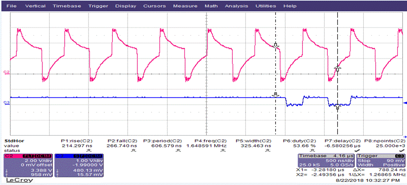
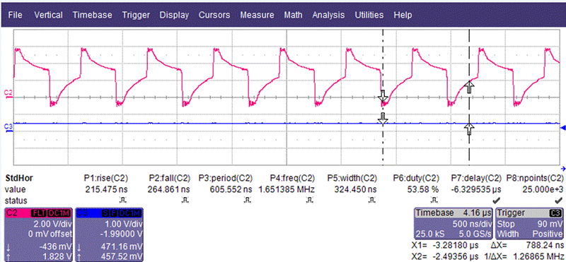
3. Changed shunt resistor value to 12ohm (Under 15ohm), PWM waveform changed as below. Is it normal operation? Is it saturation state? 

   250A current input


  300A current input


When changed Shunt resistor value to under 15ohm and 250A~300A current input, PWM waveform changed above waveforms.

Regards,

Nicky

  • Hello Nicky,

    Thanks for bringing this to our attention. We are looking over this now.

    Sincerely,
    Peter Iliya
    Current Sensing Applications
  • Nicky,

    1. Connect  VAC M4645-X080  to  DRV401 EVM.  

    We did not release a DRV401EVM.  You would need to layout your own board.  If you got some board from somewhere else please share schematic and layout so I can review.

    2. Connect 13.5V input to DRV401 EVM

    The max operating voltage of the DRV401 is 5.5V.  If there is an LDO or DC/DC please make sure the current capabilities will be large enough to drive any compensation current required and current for the field probe.

    3. Input  0A~ 300A current to M4645-X080

    4. Measure the waveform of Probe input(IS2) and PWM Output from 0A to 300A by 50A duration.

    Questions

    1. How is PWM output duty cycle change when 0A~ 300A current input to M4645-X080 with 16.5ohm Shunt resistor?  

    The PWM duty cycle should not change after everything has settled.  During a transition the PWM will change as the field probe is seeing a magnetic field and then the compensation coil is driven to compensate that.   The different resistance can change the time constant also when compensating the coil.

    2. PWM Data is  2.66V during 0A to  250A but raised to 3.36V at 300A. Is it normal?

    Are the measurements done after the AC coupling output or after the filter.  When you change the current you will change the DC load as well.

    3. Changed shunt resistor value to 12ohm (Under 15ohm), PWM waveform changed as below. Is it normal operation? Is it saturation state? 

    The PWM should follow the probe field and should be close to 50% during normal operation. 

  • Hi Javier,

    Sorry for confusing about DRV401EVM.  Just tested with customer board.

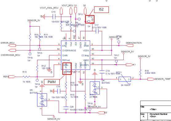
    Attached schematic, Please review it and let me get your review result.

    drv401_08_20_18_v1.pdf

    And one question.

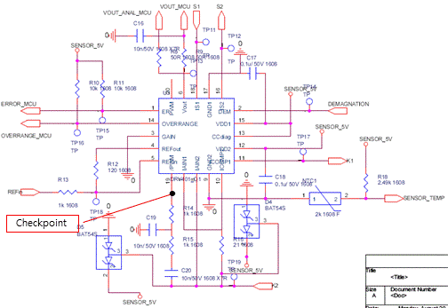
    Measure PWM voltage at below check point and its voltage level is 2.6V. Is it a normal? 

    Regards,

    Nicky

  • Hello Javier,

    Is there any update?
    Please let me get your review result ASAP.

    Thanks & Best Regards,
    Nicky
  • Nicky,

    After review I do not see an issue with the PWM connection put the signal should be a 50% duty cycle during normal operation that moves from GND to VDD.  Here is the Output expected at PWM from datasheet.

    The only time that the PWM will not get to 50% is if the compensation coil cannot completely compensate the magnetic field generated by the primary.  This can happen in two ways. 

    1. The resistance (R16 + Resistance of Compensation coil) seen at ICOMP pins is two large and the pins cannot drive the current required.  4.2V max Voltage.
    2. The current required for Compensation coil  is greater than 250mA.  Current required = Primary / #Turns Compensation Coil.

    The other Issue I saw is that D5 and D4 are connected to the same node.  One of those need to connect to the other compensation coil pin.  TP17.

  • Hi Javier,

    Have some questions about Test result as below

    1. Test Method

      - VDD = +5V

      - Primary rated current = 0A ~ 350A

      - Check pin : IS2, PWM Output

      - Shunt Resistor = 6ohm


    2. Questions

       - As you can see attached excel file, Duty cycle become longer as increase the current. Is it right?

       - When using 0.25W, 6ohm Shunt resistor, Vpwm is 5V. Is it right?

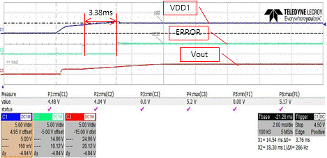
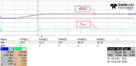
    .  - ERROR pin goes High after 3.3ms when Vdd On (please see below). What happened this time is longer than 42us?

    Regards,

    Nicky

    PWM_Wave(09_05_18).xlsx

  • Nicky,

       - As you can see attached excel file, Duty cycle become longer as increase the current. Is it right?

    Normally I would expect approximately 50% duty cycle.  Is there anyway to show the Vout at this point?  Is it saturating?  The error from 50% could only be a small offset or gain error.

       - When using 0.25W, 6ohm Shunt resistor, Vpwm is 5V. Is it right?

    During normal operations the Vpwm is a square wave and close to 50% dury cycle.  If the field probe is not compensated with the compensation coil this will change.  If the Vpwm is stuck high that means the field probe could be saturated and the IS2 pins cannot bring it out of saturation

    .  - ERROR pin goes High after 3.3ms when Vdd On (please see below). What happened this time is longer than 42us?

    This could be because the field probe is already saturated or the compensation coil is not being driven to the correct value.  This could also happen if you have a positive feedback.  An easy way to fix a positive feedback is to reverse the connection of you compensation coil or of your field probe.

  • Hi Javier,

    Normally I would expect approximately 50% duty cycle.  Is there anyway to show the Vout at this point?  Is it saturating?  The error from 50% could only be a small offset or gain error.

       -  When over 200A current asserted, duty cycle become longer than 50%. Is it saturation or not?

    This could be because the field probe is already saturated or the compensation coil is not being driven to the correct value.  This could also happen if you have a positive feedback.  An easy way to fix a positive feedback is to reverse the connection of you compensation coil or of your field probe.

       -  What means the "Positive Feedback"? Does it mean current input direction?

       -  Does "Reverse the connection" mean that connection change between IS1 and IS2 each other?  or Icomp1 and Icomp2?

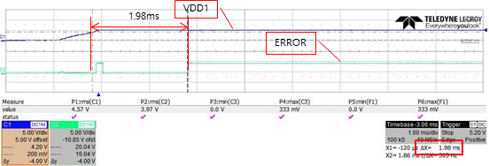
       -  Changed Shunt resistor from 16.5ohm to  5ohm,  from VDD reaches to 4V  Error pin  High timing changes from  3.38ms to 1.98ms as below. 

           Does this method is the right way to test? 

    Regards,

    Nicky

  • Nicky,

    -This could be the case that it is saturated.  Please give me the details.

    • Number of winding on compensation coil.
    • Resistance of compensation coil
    • Resistance on Rshunt
    • Voltage on VDD and any limiting factors like amount of current 

    -Positive feedback would mean that the ICOMP pins are attempting to force a current that is not in the correct direction.  It does not have to do with the primary current direction but rather in the orientation of the Icomp current relative to the probe sensing current.  For example if the field probe senses a positive field the Icomp should force a field in the opposite direction.    

    If this is an issue and it does not work and the output is always full scale then do one of the following not both. If this is occurring you should see the ERROR flag low.

    1. Switch the connection of the coil. So just reverse the connection of coil.
    2. Switch the connection of the probe.  So reverse the connection of the field probe.

    For Error pin condition please read the ERROR section on the datasheet.  With a lower Rshunt the Icomp could recover quicker giving different conditions on power up.  I would also assume your Demag pin is set low.

    For testing I would place a current on the primary and only measure the output voltage.  If the whole system is working properly you should have a linear output.  There is a limit on the current based on VDD, Power supply current limit, # winding on compensation coil,compensation coil resistance, and Rshunt.

  • Hi Javier,

    Details are as below.

    • · Number of winding on compensation coil : 1:2000
    • · Resistance of compensation coil : 16.7 ... 19.2
    • · Resistance on Rshunt : 5ohm
    • · Voltage on VDD and any limiting factors like amount of current  : VDD=5V,  Input current=230mA


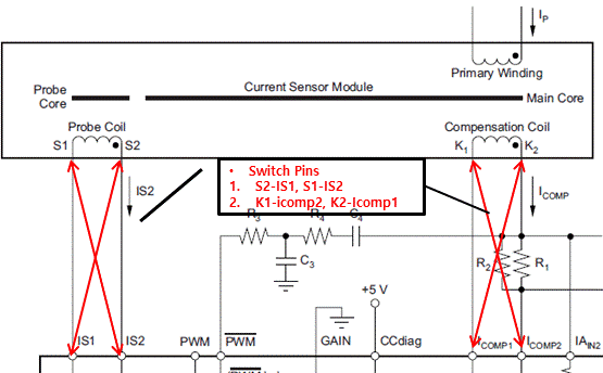
    1. Switch pins

     Currently, pin connected as Datasheet.

     But will try to test with  probe coil, Compensation coil and  DRV401-Q1 Pin connection switching as below. Is this method right?


    Please refer attached 4645-X080 datasheet for Coil specification.


    4645-X080.pdf

    Additional test result is as below. 

    1.  Input current to primary coil, and then measure the output voltage. See below waveform.

        To increase input current from 0A to 300A, ΔX get shorter. Is this result is right? 

        And get  Vout=5.08V  output and not changed even if increase the input current.  Is this output level is normal?  If not, which level is the normal? 


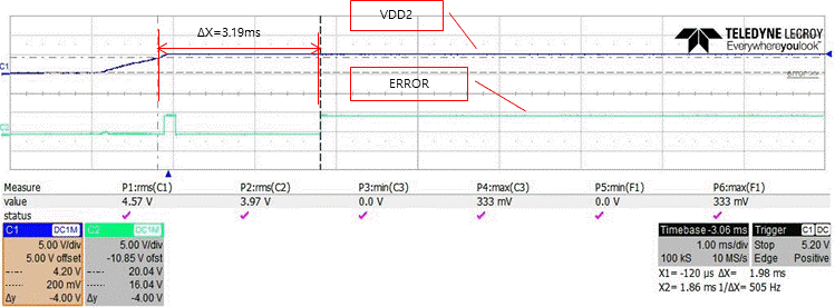
    2. Check again Error pin. To increase input current to primary coil,  ΔX get shorter. Is this result right?


     Demagnetization is not activation status.

    3. If change the direction of current input through Busbar,  output voltage level also 5V. There is no difference. Is this result right, also?

    Regards,

    Nicky

  • Nicky,

    From the conditions you gave me the max current you can measure is approximately 241A.  Please see spreadsheet attached.  The DRV401 has similar output compensation coil driver and Differential amplifier as the DRV411 and DRV421.  They have a little more data that I used for some of the assumptions. DRV401_Max_Primary_Current_Calculations_with_no_external_circuitry.xlsx

    1)I have attached a diagram for the connection.  Please only do one of the changes.  Either Option A or Option B not both.

    2)  Not sure what you are looking for in this situation.  Are you looking for the valid start time?

    3) If the part is not linear and not working If you change the current direction it should change the output and go below Vref voltage for one direction and above Vref for the other direction.

    To check the setup I would stay away from max currents.  The Vout should be equal to Vref.  If Vout is either at 0V or VDD then could have a bad connection.  This is where I would one of the connections I mentioned above.  After you verify the Vout is equal to Vref when there is no current on the primary then you can look at the output conditions works well with non railing conditions.  If it behaves linear then you can move to the start up and railing conditions.

  • Hi Javier,

    1. Test conditions

      - VDD2=5V

      - Primary current=0A

      - Temperature=25℃

      - Shunt Resistor=5ohm, 1/4W


    2. Check signals

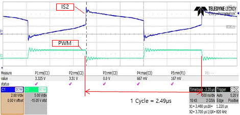
      ① PWM output

       - High : 1.270μs

       - Low : 1.220μs

       - 1cycle : 2.49μs

       - VPWM = 5.08V


      ② Error

          - Error = 5.2V

          - THIGH=60μs


      ③ Coil Driver Output

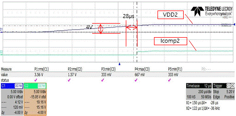
          - Vcomp2 = 2.48V

         - THIGH=28μs


    --> Question1 :  Icomp goes High after Vdd2 reaches 4V and according to datasheet, An open compensation coil is detected (longer than 100 μs)

                           What means the 100 μs? Is it the time after Vdd2 reaches 4V?

    --> Question2 : Below is the description about  Diff Amp Limitation in attached excel file.

                             Measured 2.48V without input current, even if its Limitation is 2.412V.

                             When input current to positive coil, Vcomp2 will be higher. Does it be a matter?

    Diff Amp Limitaiton

    2.412

    V

    Assumes Vref = VDD/2 and   linear function Swing high VDD-0.1V@ VDD = 3.0V and Swing high VDD-0.085V@ VDD = 5.5V. Only VDD = 5V is tested on DRV411 but similar to DRV421.   Both datasheets attached.

     ④ Reference Voltage

        - REFout = 2.6V


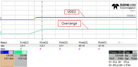
    ⑤ Over-Range

       - REFout = 5.0V


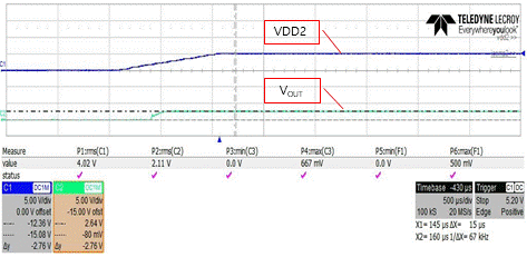
    ⑥ Output Voltage(Positive rail)

       - VOUT = 2.48V


     ⑦ Output Voltage(Negative rail)

       - VOUT = 2.48V


    --> Question3 : Measured output voltage on Positive rail and  Negative rail is  Vout=2.48V정됩니다. Is this measured voltage right?


    Regards,

    Nicky

  • Nicky,

    I appoligize for the late reply.

    --> Question1 : Icomp goes High after Vdd2 reaches 4V and according to datasheet, An open compensation coil is detected (longer than 100 μs)
    What means the 100 μs? Is it the time after Vdd2 reaches 4V?
    That is correct. The 100uS is after the part is considered on.

    --> Question2 : Below is the description about Diff Amp Limitation in attached excel file.
    Measured 2.48V without input current, even if its Limitation is 2.412V.
    When input current to positive coil, Vcomp2 will be higher. Does it be a matter?
    I need to see excel sheet be better understand your statement of limitiation.
    --> Question3 : Measured output voltage on Positive rail and Negative rail is Vout=2.48V정됩니다. Is this measured voltage right?
    I assume you are forcing the current to full scale and negative full scale? If you are overdriving the coil you may be blinding the sensor. I would ramp the current to verify the correct functionality. If this is a problem and the sensor is blinded because the field is too high the ERROR pin will get pulled low. If the Vout is not moving at all will input current I would look at your magnetic design as well to make sure it is correct.
  • Hi Javier,

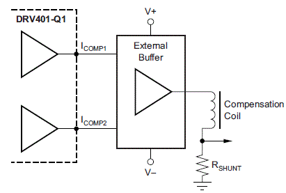
    1. External Compensation Coil Driver

       According to DRV401-Q1 Datasheet, there is description as below.

             An external driver provides a higher drive voltage and more drive current. The driver moves the power dissipation

           to the external transistors, thereby allowing a higher winding resistance in the compensation coil and more
           current.

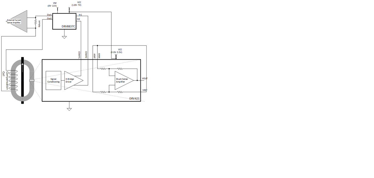
     We want to make higher current sensing circuit over 500A.

     Could you recommend external driver device or composed circuit?

    2. Demagnetization

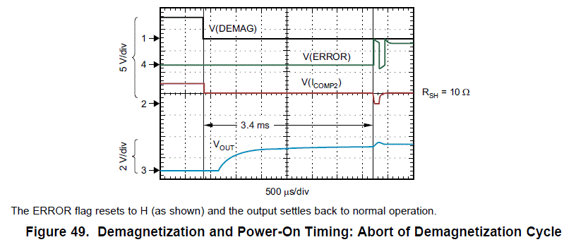
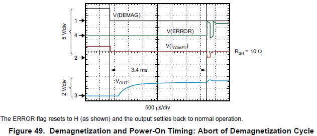
    Below waveform seems that ERROR flag resets to H and output settles back to normal operation after 3.4ms from end of Demagnetization.  

    If demagnetization is accidently stopped by external condition, Abort of Demagnetization cycle is the same with below?

    Regards,

    Nicky

  • Nicky,

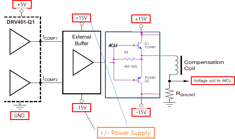
    Please see this TI Design for an example for higher output current at the output.  You may need to change the transistors to increase the current and power requirements.  Be aware of the power dissipated on the output transistors as you are increasing both the voltage and output current.

    The wave form you showed is with DEMAG pin going low and creating an abourt signal.  What is the condition of the DEMAG pin at power up?  Are you initiating the DEMAG after power up is complete?  

  • Hi Javier,

    1.  According to TI Design(), OPA237 is recommended and it uses both of  positive & negative voltage. But customer wants to use only positive voltage.

    Could you recommend other TI Design which uses only Positive voltage?

    2. Is Demagnetization of DRV401-Q1  necessary function?

        If she doesn't use this Demagnetization function, what happen?

    3. How to measure below waveform? Could you explain the procedure of this measurement?

    Regards,

    Nicky

  • Nicky,

    1.  Just change to single supply mode.  You may have issues around zero as you many not be able to compensate for any offsets.

    2.  The magnetic core could get magnetized and will get an offset from the field of a magnetized core.  You need current in both direction to demagnetize.

    3.  This is forcing the DEMAG pin low (turning of demag) during a demagnetization cycle.  This is showing that is the result of aborting a DEMAG cycle in the while it is attempting it.  One way to do this is to pulse the DEMAG pulse high for a short period of time and under 106mS (~ complete Demag cycle).

  • Hi Javier,

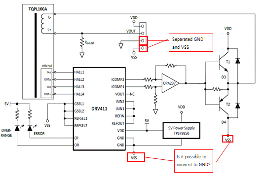
    According to tidu820 circuit, DRV411 GND pins and TR2 Vss pin are connected.

    1. Is this voltage level -15V? or just GND?

    2. In this circuit, GND and Vss are separated.

       Can this GND and Vss be connected to use single supply voltage?

    Regards,

    Nicky

  • Hi Javier,

    There are several more questions.

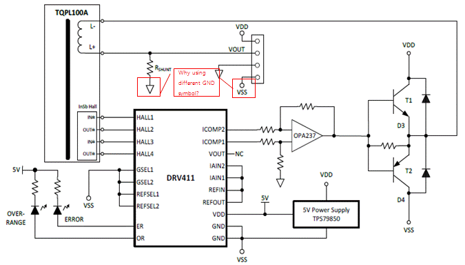
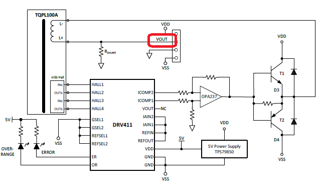
    1.  In below circuit, why different ground symbols are used? Has to separate each GND area?

    2.  Where below Vout is connected to? to MCU ?

    3. If PWM pin & Vout pin of DRV401 are not used, these pins can be left floating?

    Please let me get your answer.

    Regards,

    Nicky
  • Nicky,

    Please see replies below

    1.  In below circuit, why different ground symbols are used? Has to separate each GND area?

    VSS and GND are not the same.  This is assuming you have a dual supply like +15V, -15V and GND.

    2.  Where below Vout is connected to? to MCU ?

    This is your measurement point and can be connected to ADC, MCU or any measurement system.  Make sure the output voltage will not be larger that the input voltage of your measurement system.

    3. If PWM pin & Vout pin of DRV401 are not used, these pins can be left floating?

    Yes both these pins can be left floating.  

  • Hi Javier,

    Additional question about your answer #1.

    VSS and GND are not the same.  This is assuming you have a dual supply like +15V, -15V and GND.

    ==> If wants to use single supply voltage, can I connect Vss to GND?

           Is there any other side effect?

    Regards,

    Nicky 
  • Nicky,

    If you use the same circuit at the TI Design you will only work in one direction and you cannot measure current in both directions. Another thing is you will reach a saturation point and will not be able to get all the way to GND when there is no current flowing in the primary. Another side effect is that the degauss functionality will not work as it needs to drive current in both directions to demagnetize the core. The ICOMP pins are cable of driving current in both directions. You may need another amplifier scheme for the compensation coil drive.
  • Hi Javier,

    Make the schematic as attached.

    Could you review the schematic, and let me get the result?

    Regards,

    Nickydrv401_10_25_18_v2.pdf

  • Nicky,

    I will take an in depth review and get back to you in a couple of days.  Sorry for the delay.

  • Nicky,

    I have attached my review and made some schematic edits.

    Comments.

    Remove R18 and R20. Since you are not using the Differential amplifier the gain error correction is not required. Short RefOut to Refin.

    Differential amplifier not used so short IANI1 and IANI2 to Refout/Refin and disconnect from IComp pins. If you would like you can measure ICOMP1 and ICOMP2 but this will not tell you the current running through the compensation coil. In my opinion is not required.

    Disconnect /PWM filter connection to IAIN1. You can connect it to your measurement point to filter the same frequency. You will need to tune and make sure it is ac coupled.

    Remove D4. This should not have the transient voltages as the connection is not made directly to the compensation coil.

    Connect output of transistors to the compensation coil.

    Additional notes. Because there is no negative supply you will not be able to measure currents in both directions. Also due to this you will not be able to use the demagnetization as current needs to flow in both directions to work. Also your gain resistors R6,R7, R12, R11 are set for a gain of 4. This can be reduce gain as well.

  • Hi Javier,

    Attached revised schematic as you recommend.


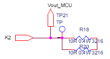
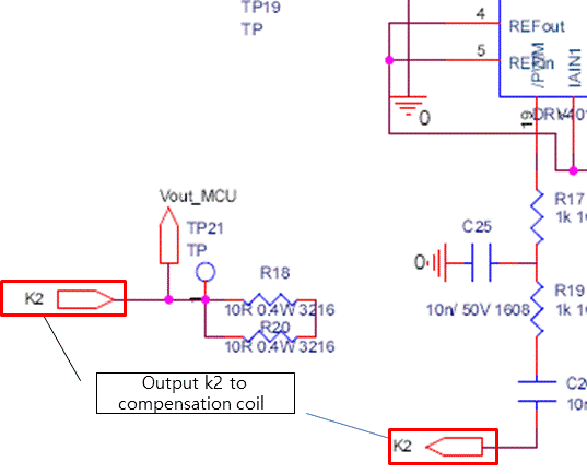
    1. Please check Output K2 connection.


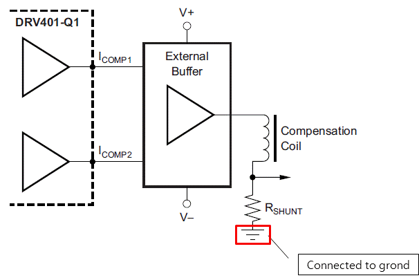
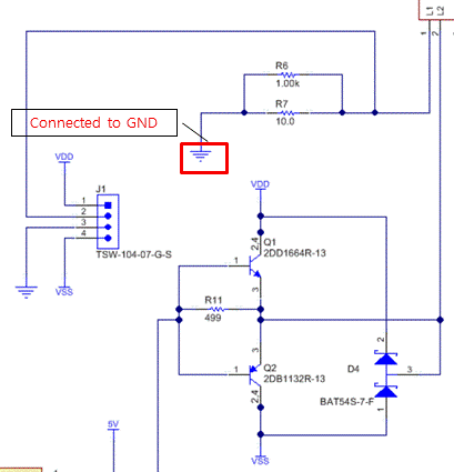
    2. Please check if shunt resistor connection to GND is right.

       According to DRV-401 Datasheet & tidu820, it connected to GND.

       ① Edited schematic


       ② External Compensation Coil Driver


    ③ tidu820 circuit


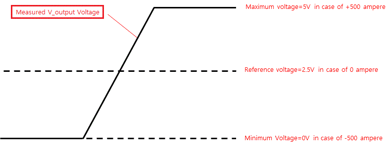
    3. Using single supply, want to make output 0~5V의 Volgate range when input +/- current to busbar as below slope.

        Is there any solution like this?


    Regards,

    Nicky
    drv401_11_07_18_v2.pdf

  • Nicky,

    If you want single supply and the current to be measure in both directions this will not work. The TI Design the output stage used dual supply.  Besides that the schematic changes look like I recommended but see item #2.

    1. Currently the connection seems correct to apply a signal to the measurement point from the PWM to counteract the noise from the switching

    2.  I do not see any connection to ground for the compensation coil.

    3.  Using single supply is more complicated where you need to supply a mid-supply current source/sink.  The other option is to increase the number of turns and make sure the resistance of the coil resistance is low enough for the DRV401 to drive the current.  This would be difficult just due to copper resistance and limitations on voltage of 5V.

  • Hi Javier,

    Decided to use dual power supply for external driver as below.

    Is there any referenced power solution for those +15V/-15V?  or Could you recommend?

    Regards,

    Nicky
  • Nicky,

    We do have a reference design that uses the +/-15V supplies.  It is here 100A Closed-Loop Current Sensor Reference Design using Bi-Polar Supplies.  I did come up with another single supply circuit but I just verified functionality.  Accuracy and noise I have not verified.  I would recommend the dual supply version but there is another option.  I used a DRV421 in my example and verification but it should work.  The downfall with my example circuit is that the bias point is not near mid-supply like the other circuit.  Like I said I would recommend dual supply vs single supply.