This thread has been locked.

If you have a related question, please click the "Ask a related question" button in the top right corner. The newly created question will be automatically linked to this question.

OPA2132: OFFSET OPA2132U

Part Number: OPA2132
Other Parts Discussed in Thread: OPA132,

Can you explain to me why with this type of schema, programmable via the ADG441 a gain of 1 or a gain of -1. We need to change the OPA2132U IC92 after a
few months of use due to off-specification output offset> 0.5μV

Ex de mesure:

Carte H447

Point mesure

Consigne

IC96-1

C404

IC92-7

1V

0.19937

0

-0.19721

-1V

0.19936

0.19936

0.20145


On the IC92-7 pin we have a difference of 0.20145-0.19721 = 4.24mV totally abnormal compared to the amp specification which gives a max offset of ± 0.5mV

  • DRUILHE,

    Is the input offset voltage changing by more than 0.5uV or 0.5mV?

    Please show the schematic of the circuit configuration you use to measure the input voltage offset.  You may not directly measure Vos with a multimeter because of  the meter's finite input impedance (1-10M) which may effect the measurement.

    You must use Insert/Attach  File link to insert  the file.

  • Sorry output offset > 0.5mV and no 0.5µV
    The measurement is made at the output of the IC92 OP pin amp 7.
    Gain -1 on measure = -0.19721
    Gain1 on measure = 0.2045
    Delta = 4.24mV
    Constant input voltage = 0.19937
  • What are the supplies, input common-mode voltage, resistor values, etc. In short, instead of describing the circuit, please show your schematic even if it's drawn by hand - picture is worth thousand words.

  • Schéma.docxSupplies +/-15V

    See attached file

  • Looking at your schematic it is clear that what changes is the output voltage with a change of the gain from 1 to -1 and this is not the same as Vos.
    What is the precision of the resistors used to set the gain?
  • Hello,
    R19=R20 = 10K 0.02% VSRJ10K000
    R635 = 4.75K 0.1% R0805
    It's not a problem of gain.
  • I am not clear how do you change the gain from +1 to -1?  Is the voltage on pin 1 of IC96 always ~0.19937V and you use IC82 to switch it between the gains?  If it's so, I don't understand why you show on the non-inerting input of IC92 (pin 6) 0V for gain 1 and 0.19936 for gain -1?  If anything, it should be opposite of what you show.  Also, to truly measure the input voltage offset, you must apply zero input (instead of 0.19937V) to both input terminals at measure the output.

    All in all, I am convinced that the error comes from the system setup and not change in OPA132 offset voltage.  If you want to confirm this, please remove OPA2132 from the board and with +/-15V supplies measure the output (Vos) in a buffer or higher gain with the input grounded - see below.

  • You forget an important point in your analysis. I hope that with this scheme the situation is clearer.
    The DG441 represents the switch by configuration of the switch the gain  change of 1 or -1
    See attached file

    PGA Problème _offset_VXI_ H447.pdf

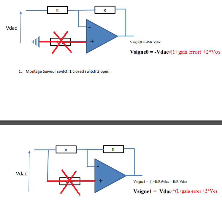
  • The inverting and non-inverting configurations ideal output voltage would be -Vdac and Vdac, respectively, but in reality must include the error due to Vos and gain error  due to mismatch of the resistors - see below text in red below.  Also, R||R equivalent resistor works to cancel the error due to IB ONLY in bipolar transistor input differential pair where input bias current has the same polarity.  Since OPA2132 uses JFET input transistors where input bias may have opposite polarity, including R||R resistor in series with the positve input terminal may double the error caused by IB instead of cancelling it - please remove it.

    Additionally, OPA2132 typical Vos is 0.5mV but the maximum  is +/-2mV, which together with gain error would account for the difference of 0.20145-0.19721 = 4.24mV you see.

  • DRUILHE

    We haven't heard back from you so we assume this answered your questions. If not just post another reply below.

    Thanks
    Dennis