This thread has been locked.

If you have a related question, please click the "Ask a related question" button in the top right corner. The newly created question will be automatically linked to this question.

INA826: Input Protection

Genius 4680 points
Part Number: INA826
Other Parts Discussed in Thread: OPA197, DRV401, INA828, TPS60403

When our cuetomer did impulse Noise test,they found attached waveform.

INA826.pptx

Vout goes to GND and then Vout returns after 5us.

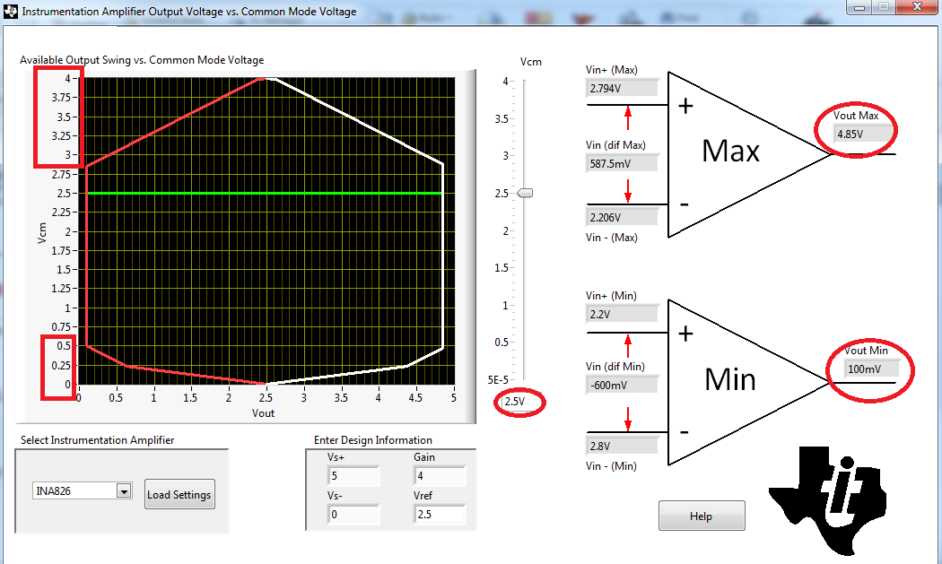
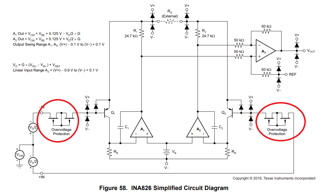
Is Cause of this behavior Input Protection of INA826 ?

When they use OPA197 in same condition,they did't find this behavior.

  • Hi Kura,

    can you show us a schematic?

    Kai
  • Kura,

    Your customer impulse "noise" seems to have a large magnitude that drives the output voltage to the negatve rail.  Once the output stage gets trioded near the ground, it takes time for it to recover from the non-linear condition - this is known as an overload recovery time.  

    Having said that, there is several unanswered questons about your customer's application - for one, the voltages shown on the attached waveforms are in hundreds of volts, which is difficult to understand.  Also, what is the input common-mode voltage of the application?  Any Vcm higher than 2.8V or lower than 0.5V would significantly limit the linear operation of the output stage - see below.

    All in all, please provide a customer schematic so we may better be able to assist you.

  • Marek-san

    Thank you for your reply.

    About circuit:

    Sorry,they can't send their circuit.

    But additinal information is here.

    They use INA826 with DRV401.

    INA826 IN+ ,IN- are connected to shunt resistor.

    REF is connected to DRV401 2.5V ref.

    Additional waveform is also attached.

    1488.Waveform.pptx

    They would like to know following.

    1.Why they did't find this behavior when they use OPA197 in same condition?

    2.If they use INA828,is this behavir seen same as INA826 ?

  • Kura-san,
    If they use DRV401 with INA826, I would expect the shunt resistor to be in front of the DRV401 and INA826 is being used to gain the signal coming out of DRV401. Therefore, in order to answer your question, I need to understand the circuit.
    1. Please provide even a hand-drawn schematic
    2. What is the input common-mode voltage (voltage on each end of the shunt resistor)?
    3. What is the output signal of DRV401? (I expect it to be fed to the input of INA826).
  • Marek-san

    Thank you for your reply.

    Hand-drawn schematic is attached

    circuit & waveform.pptxAlso, waveform of last page is OPA197..

    Currently they use INA826 +5V/0V single supply.

    1.If they use INA826 +15V/0V single supply,Is this phenomenon disappear?

    2.If they use INA828,Is this phenomenon disappear?

  • Kura-san,

    INA826 is an instrumentation amplifier with 10Gohm input impedance while OPA197 used as a difference amplifier has much lower input resistance, thus they are not equivalent circuits. Do they use resistors shown on your diagram with INA826? If so, they should not do that. The bandwidth of OPA197 is much higher than INA826, which may affect the difference between AC responses in both circuits.  Looking at the waveforms you provided, it is clear that unlike INA826 output collapsing on its negative rail, in case of OPA197 the output stays within its linear range.  Thus, I suspect that the problem your customer sees may also be related to the fact that the inputs of INA826 are overdriven beyond its linear range, which would activate input overvoltage protection circuitry (see below) causing long recovery time.

  • Kura-san

    We haven't heard back from you so we assume this answered your question. If you need more help just post another reply below.

    Thanks
    Dennis
  • Marek-san

    Thank you for your reply.
    You are correct.They don't use resistors shown on diagram with INA826.
    There is additinal information.
    When they use INA826 +12/0V single supply,this phenomenon occurred.
    When they use INA828 +12/0V single supply,this phenomenon didin't occur.

    They would like to know why this phenomenon didin't occur when they use INA828.

    Please give us your comment.
  • Thank you for your reply.
    You are correct.They don't use resistors shown on diagram with INA826.
    There is additinal information.
    When they use INA826 +12/0V single supply,this phenomenon occurred.
    When they use INA828 +12/0V single supply,this phenomenon didin't occur.

    They would like to know why this phenomenon didin't occur when they use INA828.

    Please give us your comment.

  • In order to answer your question regarding the difference in INA826 and INA828 response, I would need to have all the circuit details and conditions under which this occurs.
  • Marek-san

    Thank you for your support.

    Sorry,they can't provide schematic.
    They consider to use INA828 at +12/0V single supply,Vcm:6V
    If this phenomenon is caused by Vcm range,they can add negative power supply rail.
    Is this effective solution ?Please give us your comment.
  • Kura-san,

    In a single 12V supply, in Gain of 4 with Vref of 2.5V, INA828 has the maximum output range of 0.1V<Vout<11.9V for Vcm=6V - see below. 

    For this conditions, the valid input voltage range is shown in the diagram below to be from -0.6V to 2.35V with Vcm=6V.

  • INA828.pptxMarek-san

    Thank you for your support.

    They did experiment with the use of negative power supply for VS-.

    Please see attached file.

    Negative power supply is adjastable from GND to -12V.

    When VS- is -3V ,-5V, -12V ,inverting output is not found.

    Please let us know the reason why these waveforms are found.

    From the result of this experience,  they are cosidering to add -5V charge pump(TPS60403) to VS-.

  • Kura-san,

    I am not sure how to understand your statement of inverting input not being found - please clarify.

    Since I do not have a circuit schematic, it is not clear to me what the input current (blue trace) translates in terms of voltage and what is its common-mode voltage. Keep in mind, there is a difference in the input common-mode voltage between two inputs being single-ended vs differential.  For example for -2V and +2V inputs, Vcm=0 but for 0V, 4V inputs, Vcm=2V and NOT 0V  - Vcm is an average of two inputs.

    Using -5V negative supply instead of ground will result in the linear input voltage range shown below.  Notice, how input common-mode voltage, Vcm, is defined:  for max Vout=11.9V, Vcm=(7.175VV+4.825V)/2=6V and for min Vout=-4.9V, Vcm=(5.075V+6.925V)/2=6V

  • Sorry,my explanation was not enough.

    They are using INA828 with DRV401.INA828 REF is connected to DRV401 REFOUT(2.5V).
    Blue is impulse noise at busbar.

    There are not Input voltage waveforms in P4 to P11 of Powerpoint file.
    Input voltage of P4 to P11 are same as P1 to P3(Green).
  • Kura-san,
    The issue is that the input pulse is shown as 150A but since I do not have a schematic I have no way of knowing what does this translate into as a far as the input common-mode and differential voltage. I suspect that they violate INA828 linear input range as shown above in the plot of Output Swing vs Vcm but without reviewing a schematic I have no way to give them definite answer. Therefore, all I may say is that they should carefully review the Vout vs Vcm plot to make sure that the circuit operates within its linear range for specific supply voltages, gain and reference voltage used.

  • Kura-san

    We haven't heard back from you for a while. Did you have additional questions on this? If so, just post another reply.

    Thanks
    Dennis