Other Parts Discussed in Thread: TINA-TI, , OPA388, INA326, LM7705
Tool/software: TINA-TI or Spice Models
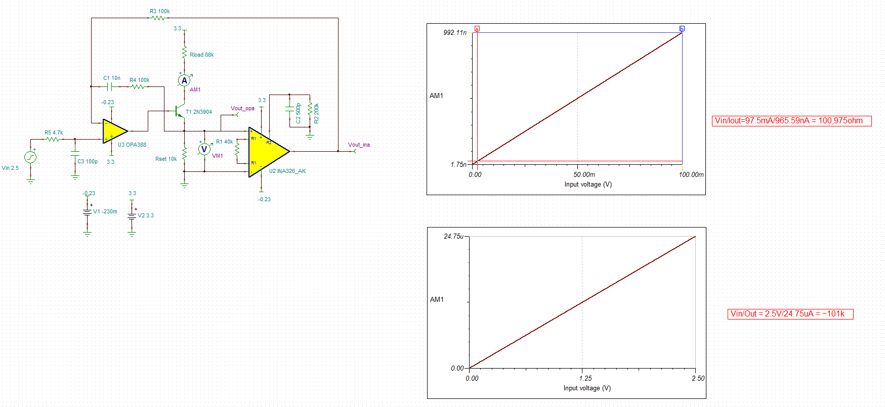
One of my design needs to source the current in nA range.
Requirement,
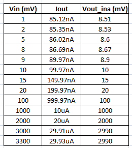
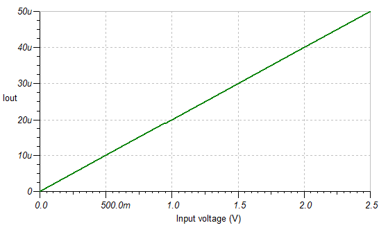
Resolution: 25nA
Accuracy: 0.1%
Range: 0 to 50uA
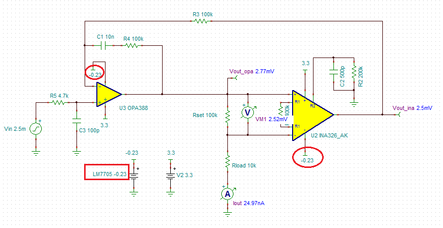
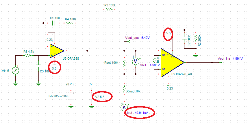
I have selected the TI parts and referred the verified design of Low level (5uA) V to I Converter by Arthur Kay.
In this design he used OP-AMP OPA333 & INA326 and simulated in TINA-TI and achieved the low current level. I am also simulated this design and able to achieve the nA current level but i had a plan to change this part to OPA388 because the voltage offset and drift.
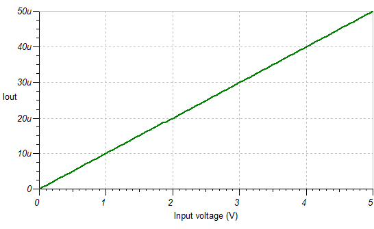
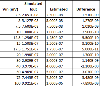
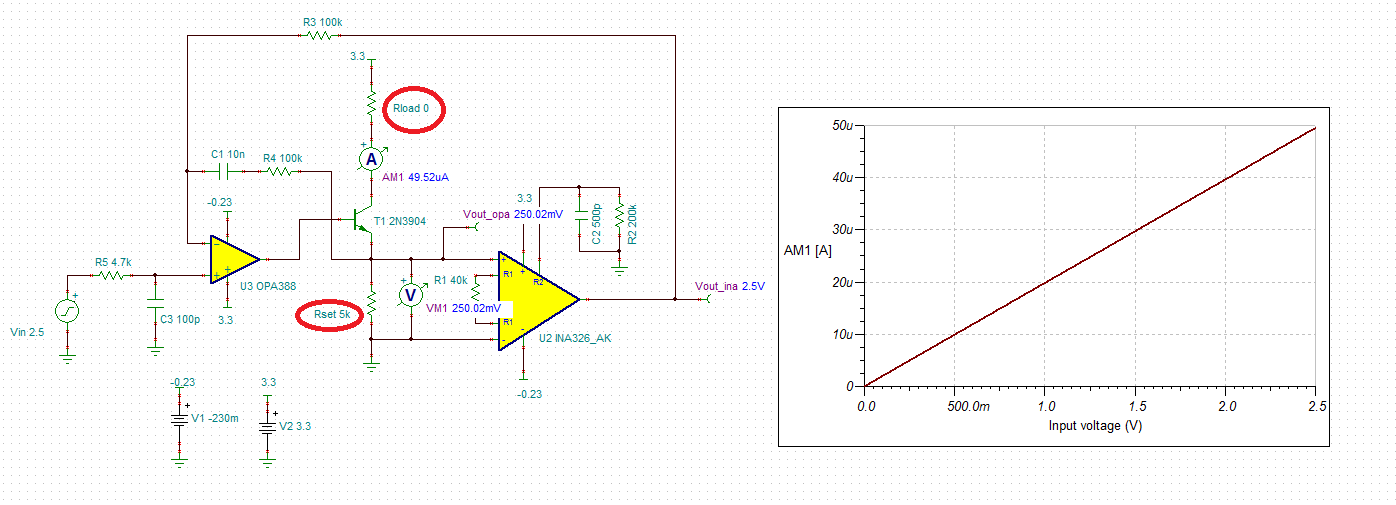
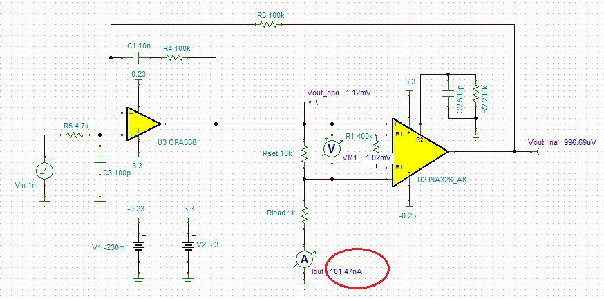
I changed to OPA388 and simulated but unable to achieve the results and the output current is non-linear.
Kindly suggest what else have to change if i want to use OPA388.