This thread has been locked.

If you have a related question, please click the "Ask a related question" button in the top right corner. The newly created question will be automatically linked to this question.

LOG114: Observed square wave at Reference current pin (I2) of LOG114

Part Number: LOG114
Other Parts Discussed in Thread: OPA335, , OPA320

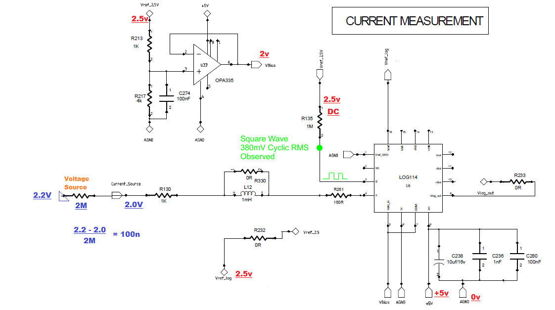
We have Observed Square Wave at reference I2 in the below circuit

Due to this we are unable to measure current less than 500nA, Is Square Wave should be on I2 or it should be DC level (VCM level)?

Kindly help to resolve the issue

  • Hi Venkatesh,

    what is the signal at the "Current_Source" pin?

    Kai
  • Hi Kai,

    It is DC current varying from 100pA to 1mA DC

    Regards,

    Venkatesh

  • Hi Venkatesh,

    yes, but because pin 4 of LOG114 sits on 2V, the "Current_Source" pin must be >2V! Have you considered that?

    Kai
  • Hi kai,

    Yes i have Considered that.

    i am appplying 2.2V as shown in below

  • Hi Venkatesh,

    is the output signal of OPA335 stable? Can you increase R213 to 10k and R217 to 40k?

    Can you increase R233 to 100R?

    Is the LOG114 powered by a clean +5V supply voltage? Or is it supplied by a noisy switcher? Does the OPA335 also have a decoupling cap?

    Another issue is stray capacitance at the inputs of LOG114. Big stray capacitances from pin 3 to GND and pin 4 to GND as it can be seen when having some cabling of longer signal lines at the input pins can destabilize the LOG114 and result in oscillation. A cure is to put R135 close to pin 3 and to put R130 (or another, bigger resistance like the 2M resistance e.g.) close to pin 4. This would isolate the stray capacitances from the input pins and restore the phase margin again.

    What is the purpose of L12, by the way? If this inductance is resonating, input currents of the wrong polarity can reach the LOG114. Take care, the LOG114 cannot handle true AC currents at the input pins 3 and 4!

    Kai

  • Hi kai klaas69,

    Thanks for your support, below are my reply to your questions.

    1) Is the output signal of OPA335 stable?

    Yes its stable. We checked it on oscilloscope.

    2)Can you increase R213 to 10k and R217 to 40k?

    We tried this. Still oscillations are observed on I2.

    3) Can you increase R233 to 100R?

    We tried this. Still oscillations are observed on I2.

    4) R135 close to pin 3?

    Yes. You can refer attached Layout.

    5)What is the purpose of L12?

    L2 is Not connected. R330 is 0Ω Also R130 is 0Ω.

    5) Is the LOG114 powered by a clean +5V supply voltage?

    We tried it with linear power supply as well as Li-ion battery, but still square wave oscillations are present on I2.

    6) Does the OPA335 also have a decoupling cap?

    No. But connected externally

    7) Obsevations:

    We have one more observation when vbias is reduced gradually, frequency  of oscillation reduces and when vbias reaches 1.35V oscillations completely disappears at I2.

    We are sending you our layout and waveform we observe at I2.

    I2 @ VBias 2V

    Layout of LOG114:

  • Hi Venkatesh,

    a 3MHz oscillation is about what I would expect, if too much stray capacitance at pin 3 and pin 4 erodes the phase margin of internal TIAs. You should minimize the signal cabling at pin 4! Increasing R281 should stop the oscillation. Could you try that? And have R281 directly mounted at pin 4!

    Kai
  • I mounted the resistor R281 close to pin 4  ( cutting off the previous trace to pin 4). I tried with values of R281 upto 2 Mohm.

    But the square wave is still observed with same frequency and amplitude.

  • Hi Venkatesh,

    the layout differs from the schematic. Can you show the full schematic?

    Kai
  • Hi kai,

    Schematic for Layout

    Regards,

    Venkatesh

  • Hi Venkatesh,

    hmm, the resistors R232, R233, R234 and R235, which is mounted and which is not? And where is V2 connected to? Very confusing. And all this additional circuitry... What is it for?

    A4 and A5 of LOG114 are no general purpose OPAmps. They should only be used for the scalings of LOG114 and only handle its internal signals.

    I would remove everything from the LOG114 which isn't urgently needed to make the LOG114 work. And be careful with any additional circuitry which increases the stray capacitance at the inputs of LOG114!

    Kai

  • Hi kai,

    We have mounted only those components as per the circuit diagram uploaded previously. We also follwoing same strategy i.e. to start working of LOG114 first. We have not mounted any other components than log114 basic circuit.  Please see below schematic NC components are not soldered on PCB.

    We have observed that when we place a capacitor (4.7uF) from I2 (pin 3) to VBias, there is no square wave oscillation at I2, but we have significant 50 Hz oscillations at output.

    You can see 50 Hz wave form at Vlogout pin 9 as below. Also we tried shielding around log114 with aluminium foil, but it does not affect the 50Hz output oscillations.

    Regards,

    Venkatesh


  • Hi Venkatesh,

    of course, it's not allowed to connect a huge capacitance from the input of TIA (pin 3 of LOG114) to AC ground (output of U33)! This will make the LOG114 stop working at all!

    Take care, with all these testings the LOG114 could have been damaged in the meanwhile and you should think about replacing the LOG114 by a fresh one.

    You should also think about running the LOG114 with a dual supply voltage, so that pin 3 and pin 4 sit on virtual GND. This can enormeously ease your current measurement.

    Cut everything from this terrible input line running to pin 4. Make a cut on the left side of R281. Increase R281 and let a current of about 500nA flow into pin 4. Best you change the circuit for a test to the circuit shown in figure 2 of datasheet.

    Take care, A3, A4 and A5 are very fast amplifiers. The whole LOG114 is fast. You cannot connect long lines and additional circuitry increasing the stray capacitance to pin 3 and pin 4. Use only the circuits and the wirings which are recommended in the datasheet.

    Kai
  • Venkatesh

    We haven't heard back from you; were you able to resolve your issue? If not just post another reply.

    Thanks
    Dennis
  • Hi Dennis,

    Issue is not yet resolved. We tried every thing. Even we ordered fresh LOG114.

    But nothing helped.

  • Hi Venkatesh,

    the LOG114 is a fast chip. You will run into trouble when connecting long lines and additional circuitry to the inputs pin 3 and pin 4 which increase the stray capacitance at these pins. Use only the circuits and the wirings which are recommended in the datasheet.

    The LOG114 is optimized for connecting photodiodes directly to the inputs, but not long cables.

    Kai
  • Also, how do you generate Vref_2.5V? Did you scope it to make sure the reference voltage is not moving?
  • Checked using scope, did not observe any noise and it is stable also
  • We have created a similar board like LOG114EVM, still we are having same problem on the board.
    Application: we are measuring leakage current by applying high voltage to insulation so we have long cable path. how can we handle this.
  • Hi Venkatesh,

    one remedy is to give the measuring current to the input of an external TIA. This TIA can be better compensated for stray capacitance at the input, because here you can add a phase lead capacitance in the feedback loop restoring the phase margin, which is not possible with the LOG114.

    Then, you can transform the output voltage of this TIA into a current by the help of a simple resistor which you mount between the TIA's output and the LOG114's input. Of course, you might need an additional inverter to correct for the 180° phase shift caused by the TIA. Or you change the polairity of measuring current. Then you only need a TIA, but not an additonal inverter. See also figure 8 and figure 9 of datasheet of LOG114.

    Whether this will work, depends on the actual stray capacitance of measuring cable and the taken OPAmp. Stray capacitance of some hundreds of pF should be able to be handled with this method. In any case you should do a phase stability anlaysis of the TIA. This needs the stray capacitance to be measured or at least to be estimated.

    Kai
  • Hello Venkatesh,

    I have been studying your LOG114 circuit to see what is different about it compared to the LOG114 single supply circuit in datasheet Fig. 2.
    We have never seen this oscillation issue you are reporting so there is certainly something different about your circuit that results in the instability. Your circuit does vary from the Fig. 2 circuit in a couple of ways and something about the differences could be leading to the oscillation you are observing at the I2 input.

    In the Fig. 2 circuit VCM, pin 5 and V- COM, pin 7, are connected together and they connect to the internal 2.5 V reference, pin 16. That is a low impedance reference output. Your circuit has pins 5 and 7 connected to the OPA335, 2V_VBIAS output. The OPA335 is a CMOS auto-zero op amp whose open-loop output impedance (Zo) is complex; especially, as frequency increases beyond the high end of its usable bandwidth. If that is the case, the impedance it presents to LOG114 pins 5 and 7 will no longer be low as it is with the internal VREF buffer pin 16. You will note that the oscillation you are observing is in the range of 3 MHz, beyond the OPA335 unity gain bandwidth.

    I suggest using the internal LOG114 VREF, pin 16, if possible. If that isn't an option, try replacing the OPA335 with a wider bandwidth, lower Zo op amp such as the OPA320. It has a 20 MHz unity-gain bandwidth and a flatter, more resistive Zo characteristic across frequency. Alternately, you could try using A4 or A5, the uncommitted op amps internal to the LOG114. Then, see if the oscillation is still present at I2.

    Regards, Thomas
    Precision Amplifiers Applications Engineering