This thread has been locked.

If you have a related question, please click the "Ask a related question" button in the top right corner. The newly created question will be automatically linked to this question.

INA301: INA301A1

Part Number: INA301
Other Parts Discussed in Thread: INA190, INA282, INA303, INA302, OPA170

I would like to know what is the input resistance to the amplifier. So that I can calcuate the effective gain of the INA with the addition of input common and differential mode filter. Also is there a application note regarding caculating the total gain and gain error due to various factors for INA301.

  • Hi,

    The impact of the external resistances on gain is explained in this datasheet by equation (5). 

    INA301 is unique in that it combines a fast amplifier with a high speed comparator. We do have other devices, such as INA190 and INA282 that enjoy minimal or no impact from external filtering. However these are relatively slow.

    Regards, Guang

  • Thanks for your reply. I was considering INA303 for its bidirectional capability. But we are using INA301 at the moment. INA301 data sheet does not give the value of the internal resistance. Can I consider the same values from INA302/INA303 datasheet, i.e for A1 12.5k and A2 5k ?

    Regards

    Dhivya

  • Hi Dhivya,

    it's not that simple. The internal bias network contributes much more to the gain error than the internal input resistance. So, knowing the internal input resistance will not help you at all.

    Kai
  • Hi Dhivya,

    INA301 and INA302/3 have identical amplifiers and resistor networks; therefore the same equation can be used for all three. The bias network effect, as Kai mentioned, has been taken into account by the equation as well.

    Regards, Guang

  • Thank you for your reply Guang. this is really helpful.
    An additional question regarding INA301.

    it has to measure currents less than 5A with a 200µOhm shunt resistor. This gives a differential input voltage at the INA301 input of less than 1mV. so with a INA gain of 20, the output of INA is 20mV which is less than the specified output swing to GND (Vgnd+30mV (max)).
    Is there a way to solve this issue, without increasing the size of the shunt?
    I was thinking of adding a small offset to one of the INA input so that the INA output is now above 30mV when current through shunt resistor is less than 5A.

    Thank you.

    Regards
    Dhivya
  • Hi Dhivya,

    the INA301A1 has an input offset voltage of up to 125µV. This would make an error of 12.5% with a signal voltage of 1mV!

    Use the INA301A3 instead and/or increase the shunt resistance.

    Kai
  • Hi Dhivya,

    Kai is correct. With INA301A3 and 1mV input differential, the output should be about 100mV, which is above the swing limit.

    The swing limit, together with offset will always pose a lower limit on the current detectable. Even with the higher gain, the minimum detectable current is 1.5A with a 200uOhm shunt.

    If it is still not acceptable, either the shunt can be increased, or a different amplifier can be chosen with higher gain, better swing and lower offset (it can be a tall order). We have amplifiers with gain of up to 1000. Here is a link to the selection tool for our analog output current sense amplifiers. You can apply filtering to zoom in on a potential candidate.

    Regards, Guang

  • Thank you for your valuable inputs Kai and Guang.

    The issue is shunt is fixed and the current range is fixed, so at the moment there is no possibility to change the shunt resolution.

    I will be using A2 with gain of 50 which has a lower input offset voltage compared to A1.

    Back to the other point I had made, how about adding an additional offset of say 15mV at the positive pin of INA. This means even when there is no current through the shunt , INA inputs have a 15mV Vsense.  This means even at low currents the INA input Vsense is 15mV or higher. This then makes the output above the swing to ground (30mV), and influence of input offset in the output error is also reduced. i.e when current through shunt is 1A, the Vsense is 200µV plus 15mV (additionally added offset to the positive input pin of INA301A2) so the output is 0,76V instead of 10mV.

    your thoughts regarding this will be really helpful . thanks in advance.

    Regards

    Dhivya

  • Hi Dhivya,

    but how do you want to implement such an input offset voltage? This would have to work for all load situations. I wouldn't do that. This is not what the INA301 is designed for.

    Kai
  • HI Kai,

    This a schematic from TINA of the Implementation of an offset to the input of INP. IN the schematic above REF is 15mV offset.

    So this offset will be present for all load conditions. It will still work for the entire range of load current, i.e from 0.1A to 250A.

  • Hi Dhivya,

    Here is my two cents.

    In theory it should work. However there are some practical aspects to consider:

    The 15mV offset is 10X bigger than the max shunt voltage. It might be challenging to extract from a large signal the much smaller useful information.

    All error sources associated with the opamp is now added directly to the INA301 input. For example, the particular opamp you selected has an offset of 2mV over temperature, which is larger than the max shunt voltage.

    The output linear swing likely is not low enough to support 15mV.

    How about INA302? A 0.75V offset can be directly applied to the REF pin so that the output is lifted off ground by the same amount. Some of the same challenges still exist, but many others are avoided.

    Regards, Guang

  • Hi Dhivya,

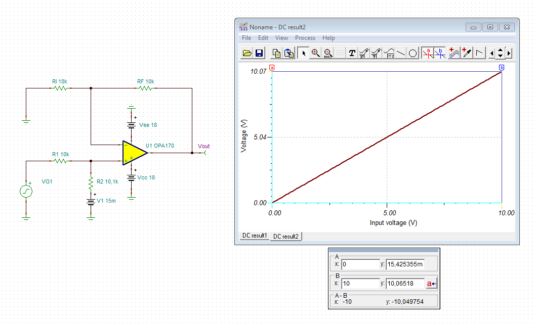
    in theory your idea might work, but not in practice, unfortunately. Your circuit suffers not only from the additional input offset voltage of OPA170, as Guang already mentioned, but also from non ideal common mode rejection caused by the imbalance of 10k resistors (R1, R12, R14 and R15). In the following simulation an error of 1% of only one of these resistors is assumed:

    The output voltage of OPA170 should be 15mV at 0V input voltage and 10.015V at 10V input voltage. But it is 15.4mV and 10.065V!

    Even with 0.1%_15ppm/°C resistors you will suffer from long term drift, making it impossible to get proper results, if your wanted signal is below 1mV.

    dhivya.TSC

    Kai

  • Thank you once again KAi and Guang.

    OPA170 was used just for simulations to see if this idea would work. I have not selected the correct opamp so far.

    As Guang mentioned, I noticed during rapid prototyping as well as simulations that error from opamp is amplified by INA301. So though it can now measure small currents there is a significant error at the output.

    I already have the simulations with INA303, which is very similar to INA302. But I had gone ahead with INA301, just due to DAC limitations for setting the voltage limits at the limit pin. Now I have to go back to using INA302 or INA303 I guess.

    Kai thank you for the simulation which shows the error caused due to imbalance in input resistors. As you mention even with high precision resistors some errors will persist .

    So in theory if my solution works it is not a good solution practically. Thank you for your time.

    One final question regarding using a reference to INA302/INA303, again for small currents the output will be close to the reference. Will this not lead to errors ? output swing ot ground is 30mV but the ina output will not reach this region for normal operating currents of (-250A to +250A). 

    So  in this case only the input offset error is significant (80µV A1 version) ?

    Sorry for the basic questions, I am trying to understand the finer point of current measurement and opamps to avoid mistakes in future design.

    Thanks again for your time.

    Regards

    Dhivya

  • Hi Dhivya,

    that's what the REF pin is made for. By applying a suited positive voltage to the REF pin you can provide an output offset voltage and shift the output voltage into the linear range.

    Kai